An automotive-grade RF front-end low noise PCB is a specialized printed circuit board designed to handle high-frequency analog signals with minimal signal degradation while withstanding the rigorous environmental standards of the automotive industry. These boards serve as the critical physical foundation for Advanced Driver Assistance Systems (ADAS), including radar, LiDAR, and V2X communication modules, where signal-to-noise ratio (SNR) directly impacts vehicle safety and decision-making latency.
Key Takeaways
- Definition: A high-reliability PCB optimized for Radio Frequency (RF) front-end circuits (LNA, PA, filters) that prioritizes low insertion loss and thermal stability.
- Critical Metric: The Noise Figure (NF) of the system is heavily influenced by the PCB substrate's Dissipation Factor (Df) and copper surface roughness.
- Misconception: High-frequency materials are not always required for every layer; hybrid stackups often balance cost and performance effectively.
- Validation Tip: Standard electrical testing is insufficient; automotive RF boards require Passive Intermodulation (PIM) testing and thermal cycling validation.
- Decision Rule: If the operating frequency exceeds 24 GHz (e.g., 77 GHz radar), standard FR4 is non-viable; PTFE or ceramic-filled hydrocarbon laminates are mandatory.
- Durability: Unlike consumer electronics, these boards must maintain RF performance after 1000+ hours of thermal shock (-40°C to +125°C).
- Manufacturing: Etching precision must be tighter than standard IPC Class 2 to maintain impedance control on narrow RF traces.
Contents
- What automotive-grade RF front-end low noise PCB really means (scope & boundaries)
- Metrics that matter (how to evaluate automotive-grade RF front-end low noise PCB)
- How to choose automotive-grade RF front-end low noise PCB (selection guidance by scenario)
- Implementation checkpoints (design to manufacturing)
- Common mistakes (and the correct approach)
- FAQ (cost, lead time, materials, testing, acceptance criteria)
- Glossary (key terms)
- Conclusion (next steps)
What Automotive-Grade RF Front-End Low Noise PCB Really Means (Scope & Boundaries)
The term "automotive-grade RF front-end low noise PCB" combines three distinct engineering disciplines: automotive reliability, RF engineering, and low-noise analog design. Understanding the boundaries of this component is essential for procurement and engineering teams.
The "RF Front-End" Scope
The RF front-end (RFFE) is the section of the circuitry located between the antenna and the digital baseband processor. In a receiver, this includes the bandpass filters, the Low Noise Amplifier (LNA), and the mixer. In a transmitter, it includes the Power Amplifier (PA).
- Function: It conditions the raw electromagnetic signal.
- Sensitivity: This stage is most susceptible to noise. Any loss or noise introduced here is amplified by subsequent stages.
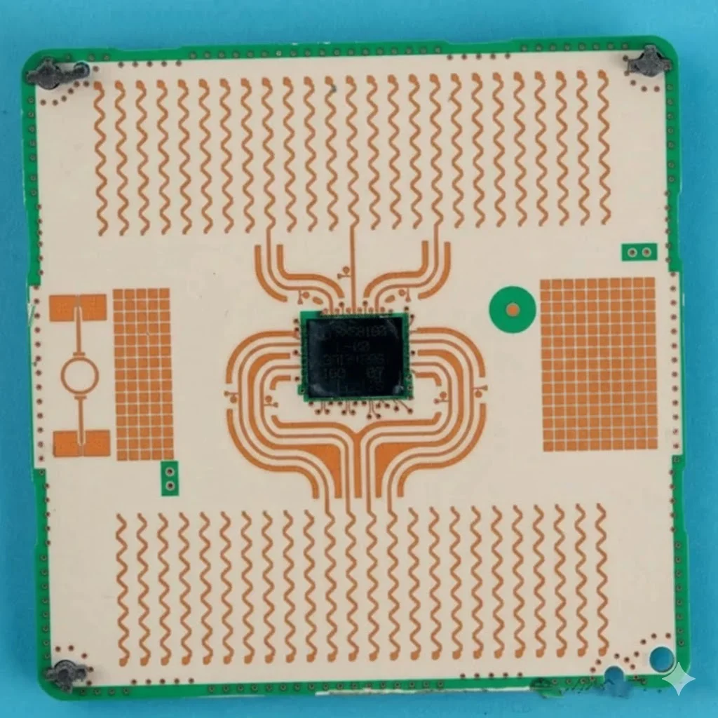
- PCB Role: The PCB acts as a transmission line. At millimeter-wave frequencies (e.g., 77 GHz for automotive radar), the PCB traces are components. A variation in trace width of just 1 mil can detune a filter or ruin impedance matching.
The "Low Noise" Requirement
Noise in a PCB context comes from three primary sources:
- Thermal Noise: Generated by the resistance of the copper traces.
- Dielectric Loss: Energy absorbed by the substrate material (converted to heat).
- Crosstalk/EMI: Interference from adjacent digital lines or power supplies.
A "low noise" PCB minimizes these factors through specific material choices (low Df), ultra-smooth copper (to reduce skin effect losses), and rigorous shielding layouts (via stitching).
The "Automotive-Grade" Boundary
This is what separates a prototype from a production unit. An industrial-grade RF front-end low noise PCB might perform identically to an automotive one on a lab bench at 25°C. However, the automotive variant must maintain that performance after:
- Thermal Shock: Rapid transitions between -40°C and +125°C (or +150°C for engine bay applications).
- Vibration: Constant mechanical stress from the vehicle's motion.
- Humidity: 85% humidity at 85°C (85/85 testing).
Automotive-grade implies compliance with AEC-Q standards for the base materials and manufacturing under IATF 16949 certified processes. It requires full traceability of every layer and laminate batch.
Metrics That Matter (How to Evaluate Automotive-Grade RF Front-End Low Noise PCB)
Evaluating an automotive-grade RF front-end low noise PCB requires looking beyond standard datasheet values. You must analyze how these metrics behave under stress and frequency.
Dielectric Constant (Dk) Stability
The Dk determines the speed of the signal and the impedance of the transmission line.
- Standard PCB: Dk can vary by ±0.2 or more.
- RF PCB: Dk tolerance must be ±0.05 or tighter.
- Thermal Coefficient of Dk (TCDk): This is critical for automotive. It measures how much Dk changes with temperature. A high TCDk means your radar might drift in frequency on a hot day, causing detection errors.
Dissipation Factor (Df)
Df measures how much signal energy is lost as heat within the substrate.
- Low Frequency: Df is negligible.
- High Frequency (77 GHz): Df is the dominant loss mechanism.
- Requirement: Automotive RF boards typically require materials with Df < 0.003 at 10 GHz.
Copper Surface Roughness
At high frequencies, the "Skin Effect" forces current to flow only on the outer surface of the conductor. If the copper surface is rough (to help it stick to the laminate), the current has to travel a longer path over the "peaks and valleys," increasing resistance and insertion loss.
- Standard Copper: High profile (rough). Good peel strength, bad for RF.
- RF Copper: VLP (Very Low Profile) or HVLP (Hyper Very Low Profile). Essential for minimizing noise and loss.
Passive Intermodulation (Pim)
PIM occurs when two signals mix in a non-linear device, creating interference. In PCBs, this can be caused by:
- Rusty or oxidized copper.
- Micro-cracks in solder joints.
- Rough etching edges.
- Automotive Impact: High PIM can desensitize the receiver, blinding the radar to small objects (like pedestrians).
Metric Comparison Table
| Metric | Standard FR4 PCB | Industrial RF PCB | Automotive RF PCB |
|---|---|---|---|
| Dk Tolerance | ± 0.20 | ± 0.05 | ± 0.04 (over temp) |
| Df (at 10 GHz) | > 0.020 | < 0.003 | < 0.003 (stable) |
| Tg (Glass Transition) | 130°C - 150°C | > 170°C | > 180°C |
| Copper Profile | Standard / Reverse Treated | Low Profile | VLP / HVLP |
| Moisture Absorption | > 0.15% | < 0.05% | < 0.02% |
| CTE (Z-axis) | 50-70 ppm/°C | 30-50 ppm/°C | < 30 ppm/°C |
| Reliability Standard | IPC Class 2 | IPC Class 2/3 | IPC Class 3 / AEC-Q |
Related resources
How to Choose Automotive-Grade RF Front-End Low Noise PCB (Selection Guidance by Scenario)
Selecting the right PCB architecture depends heavily on the specific automotive application and frequency band. Over-specifying drives up costs, while under-specifying risks safety failures.
Scenario 1: Long-Range Radar (77 Ghz)
This is the most demanding application. The signal wavelength is extremely short, making the board highly sensitive to manufacturing tolerances.
- Material: Ceramic-filled PTFE (e.g., Rogers RO3003) or specialized non-PTFE thermosets.
- Structure: Often a hybrid stackup. The top layer is the expensive RF material, while the inner layers are high-Tg FR4 for digital processing and power distribution.
- Key Constraint: Phase stability. The material must not change properties across the wide automotive temperature range.
Scenario 2: V2X Communication (5.9 Ghz)
Vehicle-to-Everything (V2X) operates at lower frequencies than radar but requires high reliability for safety messages.
- Material: Mid-loss laminates (e.g., Isola I-Tera or Panasonic Megtron 6). Pure PTFE is usually overkill and too expensive.
- Structure: Multilayer rigid board.
- Key Constraint: Cost-performance balance. Since V2X modules will be in every car, cost sensitivity is higher than for premium radar sensors.
Scenario 3: Gnss/gps Telematics (1.2 - 1.6 Ghz)
- Material: High-performance FR4 or low-loss FR4 blends.
- Structure: Standard multilayer.
- Key Constraint: Noise isolation. The challenge here is often shielding the sensitive GPS LNA from the noisy cellular (4G/5G) transmitters on the same board.
Scenario 4: In-Cabin Monitoring (60 Ghz)
Used for detecting driver fatigue or children left in cars.
- Material: Similar to long-range radar but with slightly relaxed environmental constraints (cabin is less harsh than the bumper).
- Structure: Compact HDI (High Density Interconnect) to fit in the headliner or rearview mirror.
Implementation Checkpoints (Design to Manufacturing)
Moving from a schematic to a physical automotive-grade RF front-end low noise PCB involves strict checkpoints.
1. Design Phase (DFM & Signal Integrity)
- Grounding Strategy: Use "via stitching" or "picket fences" along RF traces to contain electromagnetic fields. The distance between vias should be less than 1/8th of the wavelength at the highest operating frequency.
- Reference Planes: Ensure the RF trace has a continuous solid ground reference. Crossing a split in the ground plane creates a slot antenna, radiating noise and ruining the signal.
- Thermal Management: RF Power Amplifiers generate heat. Use thermal vias under the component pads to conduct heat to internal copper layers or a bottom heatsink. For automotive electronics PCB applications, this is critical for longevity.
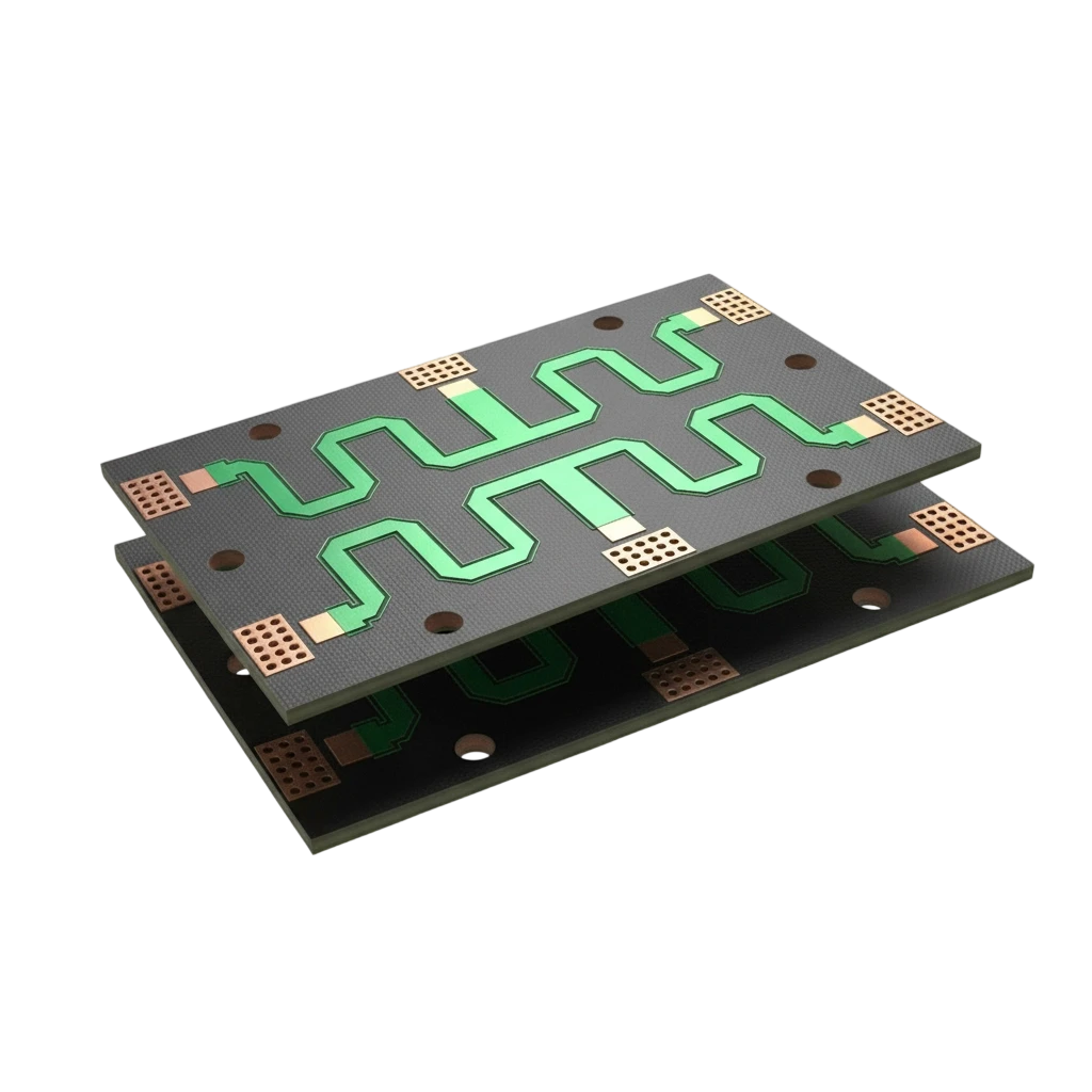
2. Material Selection & Stackup
- Hybrid Stackups: When combining PTFE and FR4, the manufacturer must manage the different Coefficients of Thermal Expansion (CTE). If not managed, the layers will delaminate during reflow soldering.
- Prepreg Selection: Use "spread glass" or "flat glass" prepregs. Standard woven glass has gaps (bundles vs. resin). If a narrow RF trace runs over a resin gap, its impedance changes compared to running over a glass bundle (Fiber Weave Effect).
3. Fabrication Process
- Etching Tolerance: Standard etching is ±10-20%. RF lines require ±5% or better. This often requires "print and etch" compensation adjustments by the CAM engineer.
- Plating: Electroless Nickel Immersion Gold (ENIG) is common, but for very high frequencies, the nickel layer is magnetic and lossy. Immersion Silver or ENEPIG (Electroless Nickel Electroless Palladium Immersion Gold) are preferred for RF front-end low noise PCB applications.
- Controlled Depth Drilling: Essential for back-drilling vias to remove stubs. Via stubs act as notch filters, reflecting signals at specific frequencies.
4. Assembly (PCBA)
- Solder Paste: Voiding under large QFN ground pads must be minimized (< 25%). Voids increase thermal resistance and RF ground inductance.
- Reflow Profile: Hybrid boards require profiles that respect the thermal limits of the FR4 while ensuring the high-thermal-mass RF components reflow properly.
- Cleanliness: Flux residues can be conductive and hygroscopic. For high-frequency PCB designs, thorough cleaning and Ionic Contamination testing are mandatory to prevent leakage currents.
Common Mistakes (and the Correct Approach)
Even experienced engineers can stumble when transitioning to automotive RF designs.
Mistake 1: Ignoring the "Fiber Weave Effect"
The Error: Routing high-speed differential pairs or RF traces parallel to the glass weave of the laminate. The Consequence: Periodic impedance variations causing signal skew and resonance. The Fix: Route traces at a 10-degree angle relative to the weave, or use spread-glass laminates where the glass bundles are flattened to minimize resin gaps.
Mistake 2: Over-Reliance on Datasheet Dk
The Error: Using the Dk value at 1 MHz or 1 GHz for a 77 GHz design. The Consequence: Incorrect impedance calculations. Dk drops as frequency increases. The Fix: Request "Design Dk" values from the laminate manufacturer specifically for your target frequency range.
Mistake 3: Poor Plating Choices
The Error: Using HASL (Hot Air Solder Leveling) for RF boards. The Consequence: Uneven surface topography ruins planarity for fine-pitch components, and the thickness variation alters the impedance of surface microstrips. The Fix: Stick to ENIG, Immersion Silver, or OSP (Organic Solderability Preservative) for flat, consistent surfaces.
Mistake 4: Neglecting the Interface
The Error: A perfect PCB design with a poor connector transition. The Consequence: High return loss (VSWR) at the connector, reflecting energy back into the amplifier. The Fix: Simulate the connector launch footprint in 3D electromagnetic software (like HFSS) and optimize the ground via placement around the connector pin.
FAQ (Cost, Lead Time, Materials, Testing, Acceptance Criteria)
Q: How much more does an automotive-grade RF PCB cost compared to a standard board? A: Typically 2x to 5x more. The cost driver is not just the RF Rogers or Taconic material, but the hybrid lamination process, tighter etching tolerances (±5%), and rigorous AEC-Q/IPC Class 3 validation testing.
Q: Can we use standard FR4 for 77 GHz automotive radar? A: No. Standard FR4 has high dielectric loss (Df > 0.02) and unstable Dk at these frequencies. The signal would be absorbed before reaching the processor. You must use PTFE or ceramic-filled hydrocarbon materials.
Q: What is the typical lead time for these boards? A: Lead times are longer, often 4-6 weeks. High-frequency laminates are often specialized stock, and the manufacturing process involves sequential lamination and complex back-drilling steps that add time.
Q: How do you validate the "Low Noise" performance in production? A: Production validation relies on TDR (Time Domain Reflectometry) for impedance coupons and occasional batch testing using a VNA (Vector Network Analyzer) to measure insertion loss on test structures. PIM testing is also used for high-power applications.
Q: What is the difference between "RF front-end low noise PCB assembly" and standard assembly? A: RF assembly requires tighter control over solder voiding (X-ray inspection is mandatory), precise placement accuracy (often < 30 microns), and specific cleaning protocols to remove flux residues that could affect RF performance.
Q: Why is "Hybrid" construction recommended? A: A hybrid stackup uses expensive RF material only for the top signal layer and cheaper FR4 for the remaining layers. This provides the necessary RF performance while significantly reducing the total material cost and improving mechanical rigidity.
Glossary (Key Terms)
| Term | Definition |
|---|---|
| AEC-Q100/200 | Automotive Electronics Council standards for stress testing active and passive components. |
| CTE (Coefficient of Thermal Expansion) | The rate at which a material expands with heat. Mismatch between copper and substrate causes failures. |
| Df (Dissipation Factor) | A measure of the energy lost as heat in the dielectric material. Lower is better for RF. |
| Dk (Dielectric Constant) | A measure of a material's ability to store electrical energy. Affects signal speed and impedance. |
| Hybrid Stackup | A PCB construction combining different materials (e.g., PTFE and FR4) into a single board. |
| Insertion Loss | The loss of signal power resulting from the insertion of a device (or trace) in a transmission line. |
| LNA (Low Noise Amplifier) | The first active component in a receiver, critical for setting the system's noise figure. |
| PIM (Passive Intermodulation) | Signal distortion caused by non-linearities in passive components (traces, connectors). |
| Skin Effect | The tendency of high-frequency current to flow only on the outer surface of a conductor. |
| TCDk | Thermal Coefficient of Dielectric Constant. Measures how Dk changes with temperature. |
| V2X | Vehicle-to-Everything communication. Allows cars to talk to infrastructure and other vehicles. |
| VLP Copper | Very Low Profile copper. Copper with minimal surface roughness to reduce skin effect losses. |
Conclusion (Next Steps)
Developing an automotive-grade RF front-end low noise PCB is a balancing act between physics, reliability, and cost. It requires a departure from standard PCB design rules, prioritizing material stability and signal integrity above all else.
For engineers and procurement managers, the path to success involves early collaboration with your manufacturer. Do not wait until the design is frozen to discuss stackups or material availability. By selecting the right hybrid materials, enforcing strict DFM guidelines, and validating with automotive-specific stress tests, you ensure your RF front-end will perform flawlessly from the prototype lab to the open road.
If you are ready to move your RF design into production or need a review of your current stackup for automotive compliance, contact our engineering team for a detailed DFM analysis.