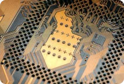
High-speed signal integrity often degrades due to unused via stubs acting as antennas. This backdrill planning guide outlines the engineering specifications, depth tolerances, and design rules required to remove these stubs effectively without compromising PCB reliability.
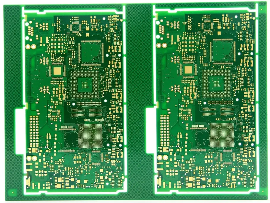
APTPCB (APTPCB PCB Factory) specializes in controlled depth drilling for high-frequency applications. Whether you are managing 56 Gbps SerDes links or optimizing PCIe Gen 5 channels, precise backdrilling is essential to minimize signal reflection and insertion loss.
Backdrill planning guide quick answer (30 seconds)
- Target Stub Length: Aim for a remaining stub length of 10 mils (0.25mm) or less. Zero stub is impossible due to mechanical tolerances; usually, 2-10 mils is the manufacturing reality.
- Drill Diameter Oversize: The backdrill tool diameter must be 8 to 10 mils (0.2mm - 0.25mm) larger than the primary plated hole to ensure all copper is removed.
- Depth Tolerance: Standard manufacturing tolerance for drill depth is ±5 mils (±0.125mm). Do not place critical copper layers within this tolerance zone.
- Clearance Zones: Copper features on layers traversed by the backdrill must have a clearance of at least 10 mils from the edge of the backdrill hole, not the original via.
- Layer Planning: Clearly define "Must Not Cut" layers in your fabrication drawing. The drill stops before reaching these layers.
- Cost Impact: Backdrilling adds 10-20% to board cost depending on the number of drill files and depth complexity.
When backdrill planning guide applies (and when it doesn’t)
Use backdrilling when:
- Signal speeds exceed 3 Gbps (or frequency > 1 GHz) where stub resonance becomes measurable.
- The PCB is thick (>2.0mm) and signals transition from top layers to upper internal layers, leaving a long stub on the bottom side.
- You need a cost-effective alternative to blind and buried vias for reducing stub length.
- Bit Error Rate (BER) is high due to deterministic jitter caused by reflections.
- You are designing complex backplanes or high-speed line cards.
Do not use backdrilling when:
- Signal speeds are low (< 1 Gbps); the cost increase is unjustified.
- The board is thin (< 1.0mm); the stub length is naturally short enough to be negligible.
- You are using a simple four layer impedance control board where signals route completely through the board (Layer 1 to Layer 4).
- High-density routing prevents the necessary clearance for the larger backdrill diameter.
- Sequential lamination (HDI) is already being used, as blind vias naturally eliminate stubs.
Backdrill planning guide rules and specifications (key parameters and limits)
Correct parameter definition is critical to prevent accidental severance of internal traces.
| Rule | Recommended Value/Range | Why it matters | How to verify | If ignored |
|---|---|---|---|---|
| Backdrill Diameter | Original Via + 0.2mm (8 mils) | Ensures complete removal of barrel plating. | Check DFM drill layer vs. plated drill layer. | Residual copper slivers cause shorts or noise. |
| Remaining Stub (Target) | 0.25mm (10 mils) max | Minimizes resonance effects. | Microsection analysis (cross-section). | Signal reflection; high insertion loss. |
| Depth Tolerance | ±0.125mm (5 mils) | Mechanical drill limitations. | Fab drawing notes. | Drilled too deep (open circuit) or too shallow (long stub). |
| Plane/Trace Clearance | Backdrill Dia + 0.25mm | Prevents drilling into adjacent circuitry. | CAD DRC (Design Rule Check). | Shorts between power planes and signal vias. |
| Must-Not-Cut Layer | Specific Layer # | Defines the stop limit for the drill. | Stackup definition in ODB++/Gerber. | Severed active signal connection. |
| Drill Aspect Ratio | < 8:1 to 10:1 | Prevents drill bit breakage/wander. | Drill table review. | Broken bits inside holes; scrapped boards. |
| Minimum Dielectric | > 0.2mm between stop layer and cut layer | Buffer for depth tolerance. | Stackup design. | Drill penetrates the "Must Not Cut" layer. |
| Backdrill Entry Side | Top or Bottom (or both) | Determines which stubs are removed. | Fab drawing view. | Wrong side drilled; stub remains. |
| Pad Removal | Remove non-functional pads on drilled layers | Reduces drill wear and debris. | Gerber layer review. | Increased burrs; potential shorts. |
| Surface Finish | Applied after backdrill | Protects exposed resin/copper. | Process flow check. | Oxidation of exposed copper at hole rim. |
Backdrill planning guide implementation steps (process checkpoints)

Follow these steps to integrate backdrilling into your design and manufacturing data.
- Identify Critical Nets: Run a signal integrity simulation to identify nets where via stubs exceed 1/10th of the signal wavelength.
- Define the Stackup: Determine the "Start Layer" and "Stop Layer" for every via type. For an 8 layer stackup example, a via connecting Layer 1 to Layer 3 will need backdrilling from Layer 8 up to Layer 4.
- Configure CAD Rules: Set up specific via types in your EDA tool (Altium, Allegro, Mentor). Assign a "Backdrill" property to these vias.
- Set Keep-Out Zones: Apply a route keep-out zone around the backdrill location on all layers that will be drilled through. Remember, the backdrill is larger than the via.
- Generate Drill Files: Output a separate NC Drill file for each backdrill depth/pair. Do not merge these with standard through-hole files.
- Create Fabrication Drawing: Explicitly list:
- Which drill file corresponds to which side.
- The "Must Not Cut" layer for each file.
- Max allowable stub length (e.g., 10 mils).
- DFM Validation: Send data to APTPCB for a pre-production check. We verify if the depth tolerance clashes with your dielectric thickness.
- First Article Inspection (FAI): Request a microsection report to verify the actual remaining stub length and depth accuracy.
Backdrill planning guide troubleshooting (failure modes and fixes)
Common issues arise from tight tolerances or incorrect data output.
Symptom: Open Circuits on High-Speed Nets
- Cause: Backdrill went too deep and cut the connection on the internal signal layer.
- Check: Verify the dielectric thickness between the signal layer and the layer below it. Is it < 5 mils?
- Fix: Increase dielectric thickness in the stackup or tighten tolerance (expensive).
- Prevention: Always leave at least 7-8 mils of dielectric buffer between the drill tip target and the active copper.
Symptom: High Bit Error Rate (BER) / Signal Loss
- Cause: Stub is still too long; backdrill was too shallow.
- Check: Review the "Must Not Cut" layer definition. Did the manufacturer play it too safe?
- Fix: Adjust the drill depth target closer to the signal layer.
- Prevention: Specify a maximum stub length (e.g., "Max 10 mils") rather than just a depth.
Symptom: Shorts to Power Planes
- Cause: Backdrill wandered and hit adjacent copper on a plane layer.
- Check: Measure the clearance (antipad) on plane layers relative to the backdrill diameter, not the via diameter.
- Fix: Increase antipad size on drilled layers.
- Prevention: Set CAD DRC to check clearances based on the oversized backdrill diameter.
Symptom: Debris in Holes
- Cause: Resin or copper shavings trapped in the via after drilling.
- Check: Visual inspection or intermittent connectivity.
- Fix: Improve cleaning/desmear process after backdrilling.
- Prevention: Ensure the manufacturer uses high-pressure wash cycles post-drill.
How to choose backdrill planning guide (design decisions and trade-offs)
Engineers often weigh backdrilling against other HDI techniques.
Backdrilling vs. Blind/Buried Vias
- Cost: Backdrilling is generally 20-40% cheaper than sequential lamination (required for blind/buried vias) because it is a subtractive process done on a standard laminated board.
- Lead Time: Backdrilling adds 1-2 days to standard lead time. Blind/buried vias can add 5-7 days due to multiple lamination cycles.
- Density: Blind vias allow routing on layers below the via. Backdrilling destroys the space through the entire drilled depth, reducing routing density.
- Reliability: Both are reliable, but backdrilling carries a slight risk of depth inaccuracy. Blind vias are mechanically robust but thermally stressful during lamination.
Backdrilling vs. Thinner PCBs
- If you can reduce board thickness, stubs naturally shrink. However, backplanes and high-layer-count boards (e.g., 20+ layers) cannot be thin. In these cases, backdrilling is the only viable option for signal integrity.
Backdrill planning guide FAQ (cost, lead time, common defects, acceptance criteria, Design for Manufacturability (DFM) files)
1. How much does backdrilling increase PCB cost? Typically, it adds 10% to 20% to the bare board cost. The price depends on the number of backdrill holes and the number of different depth setups required.
2. What is the standard lead time impact? Expect an additional 1-2 working days. This time is needed for the extra drilling cycle, cleaning, and specialized inspection (AOI/X-ray).
3. What is the minimum via size for backdrilling? We recommend a minimum original via size of 0.2mm (8 mils). Smaller vias make it difficult to align the larger backdrill bit accurately without breaking out of the capture pad.
4. Can I backdrill a connector pin hole (PTH)? Yes, this is common for press-fit connectors. However, you must ensure the remaining barrel length is sufficient to hold the connector pin securely. Usually, >1.0mm of barrel is required for mechanical retention.
5. How do I specify backdrilling in my Gerber files?
Provide a separate drill file (e.g., NCDrill_Backdrill_Top.drl). In your fabrication drawing, create a table linking this file to the specific layers it penetrates (e.g., "Drill from Top to Layer 3").
6. What is the acceptance criteria for stub length? IPC Class 2 and 3 do not have a fixed "standard" stub length; it is user-defined. A common acceptance criterion is "Stub < 0.25mm (10 mils)".
7. Does backdrilling affect impedance? Indirectly. By removing the capacitive stub, impedance discontinuity is reduced. However, the removal of ground reference planes around the hole (due to larger clearances) can slightly increase impedance at the via transition.
8. Can I use backdrilling on a four layer impedance control board? Technically yes, but it is rarely needed. On a 4-layer board, stubs are usually short (<1.6mm). It is mostly used on boards 12 layers or higher.
9. What materials are best for backdrilling? Standard FR4 is fine, but high-speed materials (like Megtron or Rogers) are usually where backdrilling is applied due to the signal speeds involved.
10. How do you verify the drill didn't cut the signal? We use electrical testing (Open/Short) after backdrilling. We also perform destructive cross-section analysis on a test coupon to verify depth accuracy before shipping.
Resources for backdrill planning guide (related pages and tools)
- High Speed PCB Manufacturing: Explore our capabilities for high-frequency laminates and controlled impedance.
- PCB Stack-up Design: Learn how to arrange layers to minimize stub lengths naturally before resorting to backdrilling.
- PCB Drilling Capabilities: Detailed specs on mechanical drilling, laser drilling, and depth tolerances.
- DFM Guidelines: Download our checklist to ensure your backdrill files are production-ready.
Backdrill planning guide glossary (key terms)
| Term | Definition |
|---|---|
| Stub | The unused portion of a plated through-hole that extends beyond the active signal layer connection. |
| Resonance | A phenomenon where the stub acts as a transmission line, reflecting signals at specific frequencies. |
| Must-Not-Cut Layer | The specific copper layer that the backdrill must stop before reaching to preserve connectivity. |
| Controlled Depth Drilling | The manufacturing process of drilling to a specific Z-axis depth, used for backdrilling and blind vias. |
| Antipad | The clearance area on a copper plane where copper is removed to prevent shorting to the via. |
| Deterministic Jitter | Timing errors in a digital signal caused by predictable factors like crosstalk or impedance mismatch (stubs). |
| Aspect Ratio | The ratio of the hole depth to the hole diameter. High aspect ratios are harder to plate and drill. |
| Press-Fit | A technology where component pins are pushed into plated holes; backdrilling must leave enough barrel for grip. |
| Insertion Loss | The loss of signal power resulting from the insertion of a device (or stub) in a transmission line. |
| Capture Pad | The copper pad surrounding the drill hole. Backdrilling often removes this on the drilled layers. |
Request a quote for backdrill planning guide
Ready to manufacture your high-speed design? APTPCB provides a comprehensive DFM review to optimize your backdrill depths and stackup for cost and reliability.
What to send for a precise quote:
- Gerber Files (RS-274X): Include separate files for backdrill layers.
- Fabrication Drawing: Clearly mark "Must Not Cut" layers and max stub tolerance.
- Stackup Details: Specify material types (e.g., Isola, Rogers) and dielectric thicknesses.
- Quantity & Lead Time: Prototype or mass production requirements.
Conclusion (next steps)
Effective backdrill planning is the bridge between theoretical signal integrity and physical manufacturing reality. By following this backdrill planning guide, defining precise "Must Not Cut" layers, and adhering to depth tolerances, you can eliminate resonance issues in your high-speed designs. APTPCB ensures your specifications are met with strict process controls, delivering reliable boards that perform exactly as simulated.