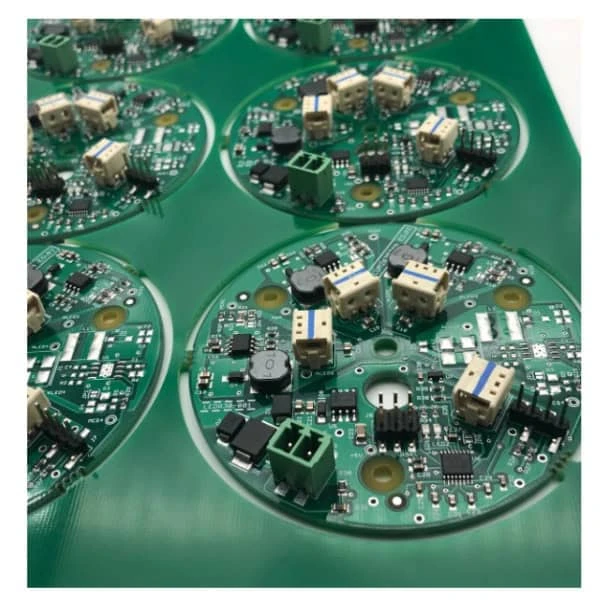
Successful BLE medical gateway PCB mass production requires a strict balance between Radio Frequency (RF) performance and medical-grade reliability. Unlike consumer electronics, medical gateways must maintain stable connectivity in electrically noisy hospital environments while adhering to safety standards like IEC 60601-1. This guide provides the engineering specifications, quality checklists, and troubleshooting protocols necessary to move your design from prototype to volume manufacturing with APTPCB (APTPCB PCB Factory).
Quick Answer (30 seconds)
For engineers launching a BLE medical gateway PCB mass production run, the following parameters are non-negotiable for yield and performance:
- Impedance Control: Maintain 50Ω ±5% on all RF traces (antenna paths) to prevent signal loss.
- Material Selection: Use High-Tg FR4 (Tg > 170°C) combined with low-loss prepreg if operating at higher frequencies or using mixed signals.
- Surface Finish: Specify ENIG (Electroless Nickel Immersion Gold) or ENEPIG for flat pads, essential for fine-pitch BGA components and wire bonding.
- Cleanliness: Adhere to IPC-6012 Class 2 or Class 3 cleanliness standards to prevent electrochemical migration (ECM) in humid medical environments.
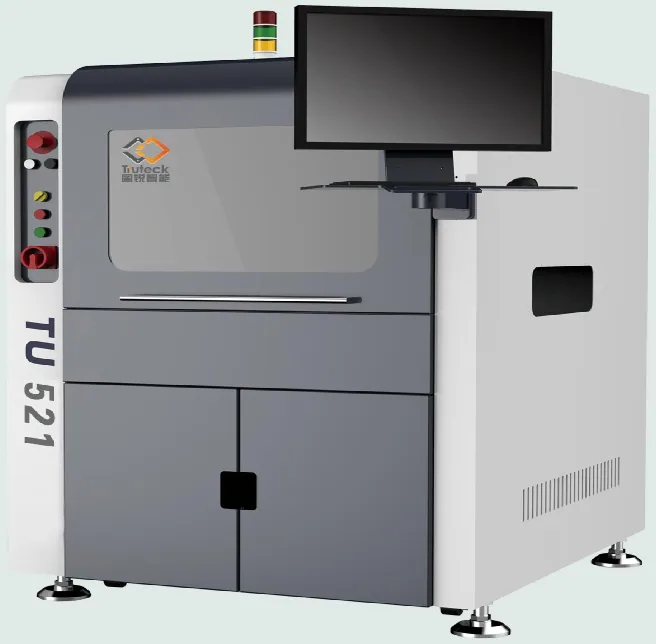
- Testing: Implement 100% Automated Optical Inspection (AOI) and X-ray inspection for QFN/BGA packages during assembly.
When BLE medical gateway PCB mass production applies (and when it doesn’t)
Understanding the scale and requirements of your project ensures you choose the right manufacturing process.
When mass production processes apply:
- Volume exceeds 500-1,000 units: Automated assembly lines and panelization become cost-effective.
- Strict Regulatory Compliance: The device requires ISO 13485 traceability and consistent IPC Class 2/3 quality for FDA or CE certification.
- Complex RF Integration: The design includes multiple radios (BLE, Wi-Fi, Cellular) requiring controlled impedance and shielding cans.
- Miniaturization: The design utilizes High-Density Interconnect (HDI) technology, such as blind or buried vias, to fit into compact enclosures.
When it does not apply (stick to prototyping):
- Proof of Concept: The circuit is not finalized, and RF tuning is still required.
- Low Volume Customization: You only need 10-50 units for clinical trials where manual inspection is feasible.
- Loose Tolerances: The device does not use wireless communication or high-speed signals (standard rigid PCBs suffice).
- Budget Constraints: The upfront tooling costs for mass production fixtures (test jigs, stencils) exceed the project budget.
Rules & specifications
To ensure a smooth transition to BLE medical gateway PCB mass production, specific design rules must be locked in before fabrication. The following table outlines critical parameters.
| Rule | Recommended Value/Range | Why it matters | How to verify | If ignored |
|---|---|---|---|---|
| Trace Impedance | 50Ω ±5% (Single-ended) | Ensures maximum power transfer from BLE chip to antenna. | TDR (Time Domain Reflectometry) coupons. | Signal reflection, reduced range, high packet loss. |
| Differential Pair | 90Ω or 100Ω ±10% | Critical for USB or Ethernet interfaces on the gateway. | Impedance Calculator & TDR test. | Data corruption, communication failure. |
| Copper Weight | 1 oz (35µm) outer / 0.5 oz inner | Balances current carrying capacity with fine line etching. | Microsection analysis. | Overheating or trace lifting during assembly. |
| Solder Mask | LPI (Liquid Photoimageable), Green/Blue | Provides insulation and prevents solder bridges. | Visual inspection (magnification). | Short circuits, especially on fine-pitch ICs. |
| Surface Finish | ENIG (2-5µin Gold over 120-240µin Nickel) | Flat surface for BGA/QFN; oxidation resistance. | XRF (X-ray Fluorescence) measurement. | Poor solder joints, "Black Pad" defect, field failure. |
| Via Structure | Filled & Capped (VIPPO) for BGA | Prevents solder theft from BGA pads. | Cross-section analysis. | BGA voids, intermittent connections. |
| Dielectric Material | High-Tg FR4 (Tg ≥ 170°C) | Resists thermal stress during reflow and operation. | Datasheet verification (e.g., Isola 370HR). | PCB delamination, barrel cracks in vias. |
| Cleanliness | < 1.56 µg/cm² NaCl equivalent | Prevents dendritic growth (shorts) in humid areas. | Ionic Contamination Test (ROSE). | Device failure after deployment in hospitals. |
| Bow & Twist | < 0.75% (IPC Class 2) | Ensures the board is flat for automated assembly. | Flatness gauge measurement. | Component misalignment, assembly machine jams. |
| Min Trace/Space | 4 mil / 4 mil (0.1mm) | Allows routing of complex BGA signals. | AOI (Automated Optical Inspection). | Shorts or opens due to etching limitations. |
| Drill Position | ±3 mil (0.075mm) | Ensures vias hit the target pads on inner layers. | X-ray alignment check. | Breakout, open circuits on inner layers. |
Implementation steps
Once the specifications are defined, the manufacturing process follows a strict sequence. APTPCB recommends the following workflow to minimize risks during BLE medical gateway PCB mass production.
Design for Manufacturing (DFM) Review
- Action: Submit Gerber files and BOM for analysis.
- Key Parameter: Check minimum trace width and spacing against factory capabilities.
- Acceptance: No critical errors reported in the DFM report.
Material Selection & Stackup Validation
- Action: Confirm the dielectric constant (Dk) and Loss Tangent (Df) for the chosen frequency (2.4 GHz for BLE).
- Key Parameter: Stackup height must fit the enclosure (e.g., 1.6mm standard).
- Acceptance: Signed stackup approval sheet.
EQ (Engineering Query) Resolution
- Action: Address any ambiguities regarding drill sizes, impedance lines, or panelization.
- Key Parameter: Clear definition of "critical nets" for RF.
- Acceptance: All EQs closed and production files locked.
Inner Layer Imaging & Etching
- Action: Transfer circuit pattern to copper laminates.
- Key Parameter: Etch factor compensation to maintain impedance width.
- Acceptance: AOI scan of inner layers showing no shorts/opens.
Lamination & Drilling
- Action: Bond layers under heat and pressure; drill vias.
- Key Parameter: Registration accuracy (layer-to-layer alignment).
- Acceptance: X-ray verification of drill alignment.
Plating & Surface Finish
- Action: Deposit copper in barrels and apply ENIG finish.
- Key Parameter: Copper thickness in hole walls (>20µm for Class 2).
- Acceptance: Non-destructive thickness measurement.
Solder Mask & Silkscreen
- Action: Apply protective mask and component legends.
- Key Parameter: Mask dam size (min 3-4 mil) between pads.
- Acceptance: Visual check for mask alignment and legibility.
Electrical Testing (E-Test)
- Action: Verify continuity and isolation.
- Key Parameter: 100% netlist testing using Flying Probe or Bed of Nails.
- Acceptance: Zero open/short circuits.
Impedance Testing
- Action: Measure test coupons on the production panel.
- Key Parameter: 50Ω ±5% verification.
- Acceptance: TDR report included with shipment.
Final QC & Packaging
- Action: Final visual inspection and vacuum packing.
- Key Parameter: Moisture Barrier Bags (MBB) with humidity indicator cards.
- Acceptance: Certificate of Compliance (CoC) issued.
Failure modes & troubleshooting
Even with rigorous planning, issues can arise. This section helps diagnose common problems in BLE medical gateway PCB mass production.
1. Symptom: Reduced BLE Range (Weak Signal)
- Causes: Impedance mismatch, incorrect stackup height, or excessive solder mask over the antenna.
- Checks: Review TDR reports; check if copper pour is too close to the antenna element.
- Fix: Adjust matching network components (inductors/capacitors); respin PCB with corrected clearance.
- Prevention: Use a Gerber Viewer to verify antenna keep-out zones before production.
2. Symptom: Intermittent Connectivity
- Causes: Microvia fracture due to thermal cycling or barrel cracking.
- Checks: Perform thermal shock testing; cross-section analysis of failed boards.
- Fix: Switch to higher Tg material; increase copper plating thickness.
- Prevention: Adhere to IPC Class 3 plating specs for medical reliability.
3. Symptom: Device Resets Randomly
- Causes: Power integrity issues; voltage drops on the 3.3V rail during TX bursts.
- Checks: Measure voltage ripple on power pins with an oscilloscope.
- Fix: Add decoupling capacitors close to the BLE SoC; increase power trace width.
- Prevention: Perform Power Integrity (PI) simulation during design.
4. Symptom: BGA/QFN Solder Bridges
- Causes: Excessive solder paste, warped PCB, or poor stencil design.
- Checks: X-ray inspection of the assembly; measure PCB flatness.
- Fix: Adjust reflow profile; use a thinner stencil or step-down stencil.
- Prevention: Enforce strict bow and twist tolerances (<0.75%).
5. Symptom: Electrochemical Migration (Dendrites)
- Causes: Ionic residue left on the board combined with humidity.
- Checks: Ionic contamination test (ROSE test).
- Fix: Improve washing process after assembly; switch to "No-Clean" flux if applicable.
- Prevention: Specify strict cleanliness limits in the fabrication notes.
6. Symptom: EMI/EMC Certification Failure
- Causes: Inadequate grounding, stitching vias missing, or noise coupling.
- Checks: Near-field probe scan to identify noise sources.
- Fix: Add shielding cans; improve ground plane continuity.
- Prevention: Follow DFM Guidelines regarding stitching vias and ground pours.
Design decisions
Strategic design choices significantly impact the success of BLE medical gateway PCB mass production.
Antenna Strategy For mass production, a PCB trace antenna is cost-effective ($0 BOM cost) but requires a larger board area and precise tuning. A chip antenna offers consistent performance and saves space but adds cost. For medical gateways in metal enclosures, an external antenna via a U.FL connector is often required to ensure signal propagation.
Layer Stackup A 4-layer board is the minimum standard for BLE gateways.
- Layer 1: Components & RF Traces.
- Layer 2: Solid Ground Plane (Critical for RF return path).
- Layer 3: Power Plane (3.3V / 5V).
- Layer 4: Routing & Non-critical signals. Using a solid ground plane immediately below the RF layer is essential for impedance control.
Panelization Medical gateways are often small. Panelizing them (e.g., 2x5 array) improves assembly efficiency. However, ensure V-cut or mouse-bites do not stress the PCB near the ceramic antenna or crystal oscillator, as mechanical stress can crack these components.
FAQ
Q1: What is the typical lead time for BLE medical gateway PCB mass production? Standard lead time is 10-15 working days for fabrication. Assembly adds another 1-2 weeks depending on component availability. Expedited services can reduce fabrication to 3-5 days.
Q2: Should I use Rogers material for BLE (2.4 GHz)? Not necessarily. For standard BLE applications, high-quality FR4 is sufficient and more cost-effective. Rogers materials are typically reserved for frequencies above 5-10 GHz or extremely low-loss requirements.
Q3: What is the difference between IPC Class 2 and Class 3 for medical gateways? Class 2 is "Dedicated Service Electronic Products" (reliable). Class 3 is "High Reliability" (life support). Most monitoring gateways fall under Class 2, but Class 3 is recommended if failure poses a critical risk.
Q4: How do I ensure my design is secure against cloning? Hardware security involves using secure elements (crypto chips) and disabling JTAG/SWD ports after programming. On the PCB side, you can bury critical traces in inner layers.
Q5: Can APTPCB handle the assembly of fine-pitch BLE SoCs? Yes. We handle BGAs with pitch down to 0.35mm and 0201 passives using high-precision pick-and-place machines and inline AOI.
Q6: How does the surface finish affect RF performance? ENIG is preferred. HASL (Hot Air Solder Leveling) has uneven thickness, which can alter the impedance of fine RF traces. Immersion Silver is good for RF but tarnishes easily.
Q7: Do I need impedance control for short RF traces? Yes. Even short traces at 2.4 GHz can act as transmission lines. If the trace length exceeds 1/10th of the wavelength, impedance control is mandatory.
Q8: What testing is required for medical PCBs? Beyond standard E-test, medical PCBs often require ionic contamination testing, microsection analysis, and 100% functional testing.
Q9: How do I manage component obsolescence? Select components with a long lifecycle status. Design the PCB with alternative footprints (dual-layout) where possible to accommodate backup parts without a board respin.
Q10: Is conformal coating necessary? If the gateway is used in a hospital environment where cleaning agents or humidity are present, conformal coating protects against corrosion and shorts.
Q11: How do I specify the color of the solder mask? White is common for medical devices to look "clean," but Green offers the best inspection contrast. Matte Black reduces light reflection but makes visual inspection harder.
Q12: Can I put vias in pads? Yes, but they must be filled and plated over (VIPPO). Open vias in pads will wick solder away, causing connection failures on the BLE module.
Glossary (key terms)
| Term | Definition | Context in BLE Gateway |
|---|---|---|
| BLE | Bluetooth Low Energy | The primary wireless protocol for low-power medical sensors. |
| Impedance | Resistance to AC current (Ohms) | Must be 50Ω for RF traces to prevent signal reflection. |
| FR4 | Flame Retardant Type 4 | The standard glass-reinforced epoxy laminate material for PCBs. |
| Tg | Glass Transition Temperature | The temperature where the PCB turns soft; High-Tg is needed for reliability. |
| AOI | Automated Optical Inspection | Camera-based inspection to find soldering defects during assembly. |
| BGA | Ball Grid Array | A type of surface-mount packaging used for high-performance BLE SoCs. |
| DFM | Design for Manufacturing | The process of designing a PCB to be easily and cheaply manufactured. |
| ECM | Electrochemical Migration | Growth of conductive filaments (dendrites) causing shorts. |
| ISM Band | Industrial, Scientific, and Medical | The 2.4 GHz radio band used by BLE and Wi-Fi. |
| IPC-6012 | Qualification and Performance Spec | The industry standard defining rigid PCB quality classes (1, 2, 3). |
| Stackup | Layer Buildup | The arrangement of copper and dielectric layers in the PCB. |
| Via | Vertical Interconnect Access | A plated hole connecting different layers of the PCB. |
Conclusion
BLE medical gateway PCB mass production is a discipline that tolerates no ambiguity. The difference between a reliable medical device and a field failure often lies in the details: the precision of the impedance, the quality of the surface finish, and the rigor of the testing process. By adhering to the specifications outlined above—specifically regarding material selection, stackup validation, and IPC standards—you ensure your product meets the demands of the healthcare industry.
Ready to validate your design for volume manufacturing? Contact APTPCB today to start your DFM review and ensure your medical gateway is built to the highest standard.