
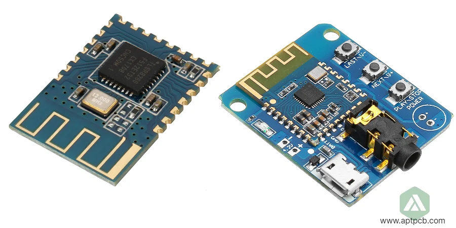
A Bluetooth PCB assembly integrates a Bluetooth radio or module, antenna, power, clocks, host interfaces and firmware into a manufacturable 2.4 GHz product. Range and connection quality depend on antenna environment, RF matching, power noise, firmware and enclosure—not on the Bluetooth version alone.
Key takeaways
- A prequalified module can reduce RF design and qualification scope but does not remove product-level regulatory work.
- Preserve the antenna manufacturer's keep-out, ground and enclosure assumptions.
- Route the RF feed as a controlled structure and include a tuning network/test access.
- Keep switch-mode power, fast clocks, displays and cables away from the antenna/current path.
- Program unique addresses/keys and firmware through a controlled traceable process.
- Define whether production test is continuity, conducted RF, over-the-air or functional connection testing.
Module versus chip-down design
| Option | Advantages | Trade-offs |
|---|---|---|
| Certified radio module | Faster RF integration, known reference design | Higher unit cost, larger footprint, module constraints |
| Chip-down SoC | Size/BOM and antenna flexibility | RF design, matching, crystal and qualification burden |
| External antenna module | Easier antenna placement outside noisy enclosure | Connector/cable cost and assembly control |
Check the module's exact qualification status, antenna restrictions and integration instructions. Changing the antenna or layout can alter what prior approvals cover.
2.4 GHz layout and antenna integration
Keep the RF feed short and referenced to a continuous ground plane. Use the stack-up-specific geometry calculated with the fabricator. Place the matching network close to the antenna or radio reference-design location and keep component options for tuning.
Avoid copper, batteries, displays, metal fasteners and cables in the antenna near field unless the antenna was designed with them. Place the final product in its enclosure before tuning; an open-board match is not the final answer.
Power, clocks and coexistence
Radio current changes rapidly during transmit/receive events. Provide local decoupling and a supply with adequate transient response. Check DC/DC switching frequency and harmonics, crystal/clock emissions and host-interface edges against the 2.4 GHz receiver sensitivity.
For Wi-Fi/Bluetooth or other 2.4 GHz radios, implement the chipset's coexistence architecture and antenna strategy. Firmware scheduling cannot fully recover poor physical isolation.
Assembly and production test
- Control moisture-sensitive radio/modules per their handling classification.
- Profile reflow using the actual board, shielding and thermal mass.
- Inspect fine-pitch/BGA/LGA joints with the appropriate method.
- Program firmware, calibration, identity and security data with traceability.
- Verify current draw, clocks, interfaces and sleep/wake behavior.
- Run conducted RF tests when a port is available or a defined OTA fixture when it is not.
- Test connection, throughput/latency and coexistence in the production enclosure.
- Preserve software version, calibration data and test limits by serial number.
| Test level | What it catches |
|---|---|
| Boundary/continuity | Opens, shorts and basic assembly faults |
| Functional connection | Firmware, host interface and basic radio operation |
| Conducted RF | TX power, frequency/error and receiver metrics at a port |
| OTA fixture | Antenna/product variation and gross detuning |
| Qualification/compliance | Bluetooth SIG and regional regulatory requirements |
Bluetooth PCBA RFQ checklist
- Bluetooth technology/features, chipset/module and reference design
- Antenna type, keep-out, matching and enclosure/mechanical model
- PCB data, stack-up, RF impedance and critical layout notes
- Power rails, battery/charger and low-power current targets
- BOM, approved alternates and lifecycle requirements
- Firmware, programming, identity/key provisioning and security handling
- Shielding, coexistence and other radios/interfaces
- AOI/X-ray, conducted RF, OTA and functional test scope
- Bluetooth qualification and regional compliance ownership
- Quantities, first article and traceability requirements
Use antenna PCB, turnkey PCB assembly and IC programming, then submit the controlled package through the PCB quotation page.
Standards and scope
- Bluetooth Core Specification — Bluetooth SIG
- Bluetooth Qualification Process — Bluetooth SIG
- IEEE 802.15.2 — Coexistence of wireless personal area networks
- IPC J-STD-001 and IPC-A-610
- IPC/JEDEC J-STD-020 and J-STD-033
Bluetooth SIG qualification/listing and regional radio approvals are separate processes. Confirm the responsibilities and final product configuration.
Bluetooth PCB assembly FAQ
Does using a certified Bluetooth module eliminate certification?
No. It can reduce scope, but the final product still needs Bluetooth qualification/listing decisions and applicable regional regulatory compliance.
Why does range fall after the board enters the enclosure?
The battery, display, metal, cables and plastic dielectric can detune or shield the antenna. Tune and validate in the final mechanical configuration.
Is a 50-ohm RF trace enough?
No. Matching components, reference continuity, antenna keep-out, launch geometry and the final environment also determine performance.
What should be programmed during assembly?
Define firmware, bootloader, calibration, Bluetooth identity and any keys/certificates, including secure handling and serial-number traceability.
Is a connection test enough for production?
It proves basic operation but may miss weak output, receiver sensitivity or antenna variation. Choose a test level based on product risk and volume.