Quick Answer (30 seconds)
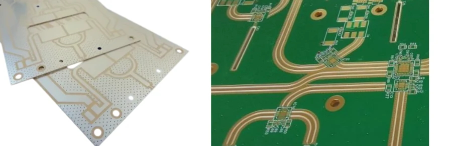
A Calibration PCB serves as a precision reference standard for test equipment, such as Vector Network Analyzers (VNAs) or an AC Power Analyzer. Unlike standard circuit boards, these require extreme stability, tight impedance control, and minimal signal loss.
- Material Stability: Use high-frequency laminates (e.g., Rogers, Taconic) with a stable Dielectric Constant (Dk) over temperature and frequency.
- Impedance Tolerance: Specify controlled impedance within ±5% or ±3% rather than the standard ±10%.
- Surface Finish: Electroless Nickel Immersion Gold (ENIG) or Hard Gold is mandatory for flat contact surfaces and oxidation resistance.
- Trace Geometry: Minimize via stubs and use back-drilling to reduce signal reflection at high frequencies.
- Connector Precision: Footprint design must match the specific connector model exactly to avoid parasitic capacitance.
- Validation: Every board requires Time Domain Reflectometry (TDR) testing before shipment.
When Calibration PCB applies (and when it doesn’t)
Understanding when to invest in high-precision manufacturing is critical for project budgeting and performance.
When to use a Calibration PCB:
- VNA Calibration Kits: You are designing Short-Open-Load-Thru (SOLT) or Thru-Reflect-Line (TRL) standards for RF measurement.
- Production Test Fixtures: The PCB acts as a "Golden Unit" to verify the pass/fail limits of an automated test system.
- Power Measurement References: You are building a reference board for an AC Power Analyzer where current path resistance must be known and stable.
- Signal Integrity Verification: You need to characterize the loss and phase delay of specific transmission lines or materials.
- Active Calibration Systems: The design includes a Calibration Generator circuit that injects precise signals for self-test routines.
When standard PCB processes suffice:
- General Logic Prototyping: If the board only carries low-speed digital signals (I2C, UART) for firmware development.
- Rough Functional Testing: When the exact amplitude or phase of a signal is less important than its simple presence.
- Low-Frequency Consumer Electronics: Devices operating below 100 MHz often do not require the expensive materials used in calibration standards.
- Disposable Breakout Boards: Simple adapters where insertion loss variations of 0.5 dB are acceptable.
Rules & specifications
To achieve metrology-grade performance, APTPCB (APTPCB PCB Factory) recommends adhering to strict design and manufacturing rules. The following table outlines the critical parameters for a Calibration PCB.
| Rule | Recommended Value/Range | Why it matters | How to verify | If ignored |
|---|---|---|---|---|
| Dielectric Constant (Dk) Tolerance | ±0.05 or better | Determines impedance accuracy and signal velocity. | Material datasheet & TDR test. | Impedance mismatch; phase errors in measurements. |
| Dissipation Factor (Df) | < 0.003 @ 10 GHz | Minimizes signal loss (insertion loss) as frequency rises. | VNA transmission test (S21). | High signal attenuation; inaccurate gain calibration. |
| Copper Surface Roughness | VLP or HVLP (Very Low Profile) | Rough copper increases skin effect losses at high frequencies. | Microsection analysis. | Higher than expected insertion loss; modeling errors. |
| Impedance Control | ±5% (Standard), ±3% (Premium) | Ensures maximum power transfer and minimizes reflections. | Impedance Calculator & TDR. | Signal reflections (Return Loss) degrade calibration accuracy. |
| Surface Finish | ENIG or Hard Gold (>30µin) | Provides a flat surface for connector seating and resists corrosion. | X-Ray Fluorescence (XRF). | Contact resistance varies; calibration drifts over time. |
| Solder Mask Registration | ±2 mil (0.05 mm) | Prevents mask from encroaching on pads, affecting soldering. | Optical inspection. | Poor connector seating; impedance discontinuities at pads. |
| Via Plating Thickness | > 25 µm (1 mil) | Ensures thermal reliability and low resistance for ground paths. | Cross-section analysis. | Via cracking during thermal cycling; unstable ground reference. |
| Trace Width Accuracy | ±10% or ±0.5 mil | Directly impacts characteristic impedance. | AOI (Automated Optical Inspection). | Impedance falls out of spec; batch-to-batch variation. |
| Weave Effect Mitigation | Spread Glass (e.g., 1067, 1078) | Prevents periodic loading effects from glass bundles. | Material specification check. | Skew in differential pairs; resonance at specific frequencies. |
| Moisture Absorption | < 0.1% | Water is polar and changes the Dk of the substrate. | Bake-out & weight test. | Electrical properties drift in humid environments. |
| Thermal Expansion (z-axis) | < 50 ppm/°C | Prevents barrel cracks and pad lifting during soldering. | TMA (Thermomechanical Analysis). | Board failure after reflow or during temperature cycling. |
Implementation steps

Designing a Calibration PCB requires a systematic approach that prioritizes physical accuracy over component density.
Define the Frequency Range: Determine the upper frequency limit (e.g., 6 GHz, 20 GHz, 40 GHz). This dictates the material selection. For frequencies above 1 GHz, standard FR4 is often insufficient.
Select the Substrate Material: Choose a laminate with low Df and stable Dk. APTPCB often suggests Rogers series for RF calibration boards due to their consistency.
Design the Stackup: Calculate trace widths for 50-ohm (or required) impedance. Ensure reference planes are solid copper. Avoid split planes under critical signal paths to prevent return path discontinuities.
Optimize Connector Footprints: Do not rely on default CAD library footprints. Request the manufacturer's recommended high-frequency footprint. Use "anti-pads" (cutouts in ground planes) to match the impedance of the connector pin transition.
Route Critical Traces: Keep calibration traces as short as possible. If designing a "Thru" line, ensure it is a straight line. Avoid vias on the signal path if possible. If vias are needed, use back-drilling to remove stubs.
Add Grounding Vias: Stitch the ground planes with vias along the signal path (via fencing). The spacing should be less than $\lambda/20$ of the highest operating frequency to prevent resonance.
Fabrication Data Generation: Export Gerber files with high resolution. Include a drill table that specifies finished hole sizes. Clearly mark "Controlled Impedance" requirements in the fabrication notes.
Post-Fab Verification: Upon receiving the bare boards, perform a visual inspection of the trace edges. Use a TDR to verify impedance before assembling expensive connectors.
Assembly and Cleaning: Solder connectors using a precision profile. Flux residue can be conductive or capacitive at high frequencies; ensure thorough cleaning.
Final Characterization: Measure the S-parameters (S11, S21) of the finished Calibration PCB. Store this data as the "correction file" for the end-user.
Failure modes & troubleshooting
Even with a perfect design, issues can arise during fabrication or usage. The following table helps diagnose common failures in Calibration PCBs.
Symptom: Impedance is consistently lower than designed.
- Causes: Trace width is too wide (over-etching issues), or dielectric thickness is thinner than specified (lamination pressure).
- Checks: Measure trace width with a microscope. Check stackup report from the fab house.
- Fix: Adjust design trace width for the next revision.
- Prevention: Use DFM Guidelines to set realistic etching tolerances.
Symptom: High Insertion Loss at high frequencies.
- Causes: Material Df is too high, copper is too rough, or plating issues (e.g., nickel resonance).
- Checks: Verify material type. Check if ENIG nickel layer is affecting RF signals (magnetic properties).
- Fix: Switch to Silver immersion or OSP for very high frequencies (>20 GHz).
- Prevention: Specify "VLP Copper" and appropriate surface finish in fab notes.
Symptom: Measurement drift over time.
- Causes: Moisture absorption, oxidation of contacts, or mechanical stress on connectors.
- Checks: Bake the board to remove moisture. Inspect connectors for wear.
- Fix: Store calibration boards in a desiccator. Replace worn connectors.
- Prevention: Use low-hygroscopic materials (e.g., PTFE-based).
Symptom: Ripples in S-parameter data (Resonance).
- Causes: Ground via spacing is too large, or stub resonance from non-back-drilled vias.
- Checks: Calculate resonant frequency of via stubs. Check ground stitching distance.
- Fix: Back-drill vias or use blind/buried vias.
- Prevention: Simulate the transition from connector to PCB in 3D EM software.
Symptom: Poor repeatability of connections.
- Causes: Connector torque variation, surface finish unevenness, or pad lifting.
- Checks: Use a torque wrench. Inspect pad flatness.
- Fix: Re-solder or replace the board if pads are damaged.
- Prevention: Use larger pads or teardrops for mechanical strength; ensure ENIG finish.
Symptom: Thermal drift during operation.
- Causes: High Coefficient of Thermal Expansion (CTE) of the material.
- Checks: Heat the board and monitor impedance change.
- Fix: Use ceramic-filled laminates with low CTE.
- Prevention: Select materials stable across the operating temperature range.
Design decisions
When finalizing the layout, specific architectural decisions impact the utility of the Calibration PCB.
Connector Placement: For VNA calibration kits, place connectors far enough apart to allow the user to attach cables without mechanical interference. However, keep them close enough to minimize board size and warping.
The "Calibration Generator" Integration: Some advanced calibration boards include an active Calibration Generator. This circuit generates a known pulse or frequency comb. If your design includes this:
- Isolate the power supply of the generator from the reference traces.
- Shield the generator section to prevent radiation from coupling into the calibration standards.
- Use thermal reliefs carefully; the generator generates heat which can alter the Dk of nearby traces.
AC Power Analyzer Standards: For boards used to calibrate an AC Power Analyzer:
- Trace thickness (copper weight) is critical. Use 2oz or 3oz copper to handle current without heating.
- Use Kelvin connections (4-wire sensing) for current sense resistors.
- Ensure high voltage isolation (creepage and clearance) between phases.
FAQ
Q: Why is ENIG preferred over HASL for Calibration PCBs? A: HASL (Hot Air Solder Leveling) leaves an uneven surface, which causes connector misalignment and impedance variations. ENIG provides a perfectly flat surface essential for high-frequency contact.
Q: Can I use FR4 for a Calibration PCB? A: Only for low frequencies (typically < 500 MHz) or DC applications. FR4 has a variable Dk and high loss, making it unsuitable for precision RF or high-speed digital calibration.
Q: What is the typical lead time for these boards? A: Due to specialized materials (like Rogers or Taconic) and precise etching requirements, lead times are typically 5-10 days. APTPCB can expedite this if materials are in stock.
Q: How often should a Calibration PCB be replaced? A: It depends on usage. Connectors wear out after a few hundred mating cycles. If the gold plating on the pads wears through, the impedance will change, and the board should be replaced.
Q: Do I need back-drilling for all vias? A: Not for all. Back-drilling is required for high-speed signal vias to remove the unused "stub" portion that acts as an antenna or capacitor. Ground stitching vias do not need back-drilling.
Q: What is the cost difference between standard and calibration-grade PCBs? A: Calibration-grade boards can cost 2-5x more due to expensive laminates, tighter tolerance controls (±5% impedance), and advanced inspection requirements (TDR, cross-sectioning).
Q: How does copper roughness affect the calibration? A: At high frequencies, current flows on the skin of the conductor. Rough copper increases the effective path length, increasing resistance and insertion loss, which distorts calibration data.
Q: Can I combine a Calibration Generator and passive standards on one board? A: Yes, but isolation is key. Ensure the active circuitry does not introduce noise into the passive reference lines. Use separate ground planes joined at a single point (star ground).
Q: What is the "Open" standard in a PCB calibration kit? A: It is not just a cut trace. It must be a designed open circuit that accounts for the fringing capacitance at the end of the line. This capacitance must be modeled and provided to the VNA.
Q: How do I specify the material to the manufacturer? A: Do not just say "Rogers." Specify the exact series (e.g., RO4350B), thickness (e.g., 20 mil), and copper weight (e.g., 0.5 oz).
Q: Why is the "Thru" line length important? A: In TRL calibration, the length of the line determines the frequency band where the calibration is valid. You may need multiple lines for broadband calibration.
Q: Does solder mask affect impedance? A: Yes. Solder mask adds dielectric material on top of the trace, lowering the impedance by 2-3 ohms. Calculations must account for the mask's presence and Dk.
Related pages & tools
- Material Selection: Rogers PCB Materials
- Manufacturing Capabilities: PCB Manufacturing Services
- Design Verification: Free Gerber Viewer
Glossary (key terms)
| Term | Definition |
|---|---|
| SOLT | Short-Open-Load-Thru. A common calibration method for VNAs using four known standards. |
| TRL | Thru-Reflect-Line. A highly accurate calibration method often used for on-wafer or PCB measurements. |
| De-embedding | The mathematical process of removing the effects of fixtures or connectors from the measurement data. |
| Characteristic Impedance | The ratio of voltage to current for a wave propagating along a transmission line (usually 50Ω). |
| Return Loss (S11) | The amount of signal reflected back to the source due to impedance mismatch. |
| Insertion Loss (S21) | The amount of signal lost as it travels through the transmission line. |
| Skin Effect | The tendency of high-frequency alternating current to flow near the surface of the conductor. |
| Dielectric Absorption | The retention of charge by the dielectric material, which can affect precision measurements. |
| Fiducial Marker | A copper mark used by assembly machines to optically align the PCB. |
| CTE | Coefficient of Thermal Expansion. The rate at which a material expands with heat. |
| Back-drilling | A manufacturing process to remove the unused portion of a plated through-hole (via stub). |
| Golden Unit | A reference PCB known to be good, used to validate test systems. |
Conclusion
Designing a Calibration PCB is an exercise in precision. Every micron of copper and every degree of temperature affects the result. By selecting the right materials, enforcing strict impedance controls, and validating with TDR, you ensure your test equipment remains accurate.
Whether you are building a custom Calibration Generator or a passive reference kit, APTPCB provides the engineering support and manufacturing precision required for metrology-grade boards. Ensure your specifications are clear, and verify your design files before production to minimize costly iterations.