Key Takeaways
- Definition: A CAN Transceiver PCB is a printed circuit board specifically designed to host the physical layer interface (PHY) between a CAN controller and the two-wire differential bus network.
- Impedance Control: The most critical metric is maintaining a differential impedance of 120 Ohms (±10%) to prevent signal reflection and data corruption.
- CAN FD Evolution: Modern designs often require CAN FD PCB layouts, which handle higher data rates (up to 5-8 Mbps) and demand stricter signal integrity than classical CAN.
- Protection: Effective layouts must integrate transient voltage suppression (TVS) and common-mode chokes without disrupting the differential pair geometry.
- Misconception: Many designers believe any FR4 material works; however, high-temperature automotive environments often require High-Tg materials to prevent delamination.
- Validation: Acceptance relies on Time Domain Reflectometry (TDR) testing to verify impedance profiles before component assembly.
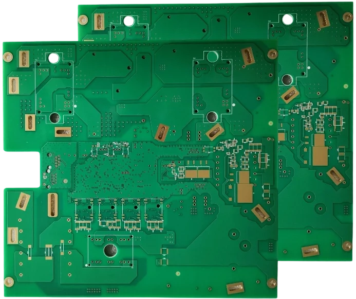
- Manufacturing: APTPCB (APTPCB PCB Factory) recommends verifying stackup capabilities early to ensure the dielectric thickness supports the required trace widths.
What is the first step toward a successful build. While Controller Area Network (CAN) Transceiver PCB really means (scope & boundaries)
Understanding the core requirements of a CAN Transceiver PCB is the first step toward a successful build. While the Controller Area Network (CAN) is a communication protocol, the PCB is the physical medium that ensures this protocol functions correctly under electrical stress.
A CAN Transceiver PCB acts as the bridge between the digital logic of a microcontroller and the harsh analog environment of the bus cabling. It is not merely a carrier for the transceiver chip; it is an active component in the signal chain. The layout must manage differential signaling (CAN_H and CAN_L), ensuring that external noise is rejected and that the board itself does not emit electromagnetic interference (EMI).
In modern applications, the scope has expanded. We now see CAN FD PCB (Flexible Data-rate) designs that require tighter tolerances than standard ISO 11898 implementations. Furthermore, in complex automotive sensor suites, a CAN node might coexist on the same board as a Radar Transceiver PCB or an Optical Transceiver PCB, requiring careful isolation strategies to prevent cross-talk between high-frequency radar signals and the lower-frequency CAN bus.
is the first step toward a successful build. While Controller Area Network (CAN) Transceiver PCB metrics that matter (how to evaluate quality)
Once the scope is defined, engineers must quantify quality using specific metrics. These parameters determine whether a board will perform reliably in the field or fail during EMC testing.
| Metric | Why it matters | Typical Range / Factors | How to measure |
|---|---|---|---|
| Differential Impedance | Matches the characteristic impedance of the cable to stop signal reflections (ringing). | 120 Ohms ±10%. Influenced by trace width, spacing, and dielectric height. | Time Domain Reflectometry (TDR) coupons or in-circuit testing. |
| Common Mode Rejection | Determines the board's ability to ignore noise affecting both lines equally. | > 60dB typical. Influenced by symmetry of the differential pair layout. | Vector Network Analyzer (VNA) or oscilloscope math functions. |
| DC Resistance (DCR) | High resistance causes voltage drops, potentially pushing signals below the recessive/dominant thresholds. | < 100 mΩ for short runs. Depends on copper weight (1oz vs 2oz). | 4-wire Kelvin resistance measurement. |
| Dielectric Breakdown | Critical for isolated CAN transceivers in EVs or high-voltage industrial systems. | > 2kV for galvanic isolation zones. Depends on creepage/clearance distance. | Hi-Pot (High Potential) testing. |
| Thermal Resistance (Rth) | The transceiver chip can get hot; the PCB must dissipate this heat to prevent thermal shutdown. | Depends on copper area connected to the thermal pad (if present). | Thermal imaging or thermocouple during load testing. |
| Skew | The time difference between CAN_H and CAN_L signals. High skew converts differential signals into common-mode noise. | < 100 ps. Controlled by length matching the traces exactly. | High-speed oscilloscope. |
How to choose is the first step toward a successful build. While Controller Area Network (CAN) Transceiver PCB: selection guidance by scenario (trade-offs)
Metrics provide the data, but the application environment dictates the design choices. Below are common scenarios and how to choose the right CAN Transceiver PCB configuration for each.
1. Automotive Powertrain (High Heat & Vibration)
- Requirement: Extreme reliability under thermal cycling (-40°C to +125°C).
- Trade-off: You must trade cost for durability. Standard FR4 is insufficient.
- Selection: Choose High-Tg (Glass Transition Temperature) materials (>170°C). Use heavy copper (2oz) if the board also carries power.
- APTPCB suggests: Automotive Electronics PCB standards usually apply here, requiring IPC Class 3 validation.
2. Electric Vehicle (EV) Battery Management (High Voltage)
- Requirement: Galvanic isolation to protect low-voltage logic from high-voltage battery packs.
- Trade-off: Requires larger board area for creepage and clearance slots.
- Selection: Select a layout that physically separates the transceiver side (bus side) from the MCU side. Use isolated CAN transceiver footprints and ensure no internal planes cross the isolation barrier.
3. Industrial Automation (Long Distance)
- Requirement: Signal integrity over cable runs exceeding 40 meters.
- Trade-off: Signal speed vs. distance. Lower baud rates allow longer distances, but the PCB must minimize insertion loss.
- Selection: Prioritize lower dielectric loss materials if the bus is heavily loaded. Ensure robust termination resistor placement directly at the connector.
4. Compact Robotics (Space Constrained)
- Requirement: Fitting a CAN node into a joint or actuator arm.
- Trade-off: Size vs. EMI performance. Small boards make it harder to route differential pairs away from noisy motor drivers.
- Selection: Use HDI (High Density Interconnect) techniques or Rigid-Flex designs to fold the board into the housing.
- Resource: Explore Rigid-Flex PCB capabilities for dynamic applications.
5. Consumer Electronics (Cost Sensitive)
- Requirement: Basic connectivity for smart home devices.
- Trade-off: Performance vs. Price.
- Selection: Standard FR4 (Tg 130-140), 1oz copper, standard 2-layer or 4-layer stackup. Impedance control is still necessary but tolerances can sometimes be looser if cable runs are very short (<1m).
6. High-Speed Data Logging (CAN FD)
- Requirement: Handling 5 Mbps to 8 Mbps data phases.
- Trade-off: Design complexity vs. Data throughput.
- Selection: Treat this as a High Speed PCB. Stubs must be virtually eliminated. Vias on the differential pair should be back-drilled or minimized.
is the first step toward a successful build. While Controller Area Network (CAN) Transceiver PCB implementation checkpoints (design to manufacturing)

Moving from selection to implementation requires a disciplined approach. Use this checklist to ensure your CAN Transceiver PCB design is ready for manufacturing.
- Stackup Verification: Before routing, confirm with the manufacturer that your desired trace width yields 120Ω differential impedance on the selected layer stack.
- Risk: Redesign required if traces are too thin (unetchable) or too wide (space violation).
- Acceptance: Manufacturer-approved stackup sheet.
- Placement Strategy: Place the transceiver chip as close to the connector as possible.
- Risk: Long traces between the connector and transceiver act as antennas for EMI.
- Acceptance: Distance < 20mm is a good target.
- Differential Pair Routing: Route CAN_H and CAN_L parallel to each other with constant spacing.
- Risk: Impedance discontinuities causing reflections.
- Acceptance: Visual inspection; no split planes under the pair.
- Stub Management: Minimize the length of traces connecting the transceiver pin to the main bus line (if the board is a tap).
- Risk: Stubs create signal reflections that degrade the eye diagram.
- Acceptance: Stubs should be < 0.3 meters (system level), but on-PCB stubs should be negligible.
- Grounding: Provide a solid ground reference plane immediately adjacent to the signal layer.
- Risk: Poor return path increases loop area and radiated emissions.
- Acceptance: Solid copper pour without fragmentation under signals.
- Protection Components: Place TVS diodes and Common Mode Chokes (CMC) close to the connector.
- Risk: ESD strikes destroying the transceiver.
- Acceptance: Components placed in the direct signal path (no stubs to protection devices).
- Termination: If this is an end node, include a 120Ω resistor.
- Risk: Missing termination causes total bus failure.
- Acceptance: BOM verification and footprint check.
- Decoupling Capacitors: Place 100nF capacitors close to the transceiver power pins.
- Risk: Voltage sags during dominant state transmission.
- Acceptance: Capacitor within 2-3mm of the VCC pin.
- Silkscreen Markings: Clearly label CAN_H, CAN_L, and GND.
- Risk: Field wiring errors.
- Acceptance: Legible text near the connector.
- DFM Review: Run a Design for Manufacturing check.
- Risk: Production delays due to drill-to-copper violations.
- Acceptance: Pass report from DFM Guidelines.
is the first step toward a successful build. While Controller Area Network (CAN) Transceiver PCB common mistakes (and the correct approach)
Even experienced engineers can overlook details that compromise a Bus Transceiver PCB. Here are the most frequent errors and how to fix them.
- Mistake: Splitting the reference plane.
- Correction: Never route differential pairs over a gap in the ground plane (e.g., a split between analog and digital ground). This destroys impedance and creates a slot antenna. Always route over solid copper.
- Mistake: Ignoring the "Split Termination" option.
- Correction: Instead of a single 120Ω resistor, use two 60Ω resistors in series with a capacitor to ground in the middle. This acts as a low-pass filter for common-mode noise, improving EMC performance significantly.
- Mistake: Excessive via usage.
- Correction: Every via adds inductance and impedance discontinuity. Route the differential pair on a single layer from transceiver to connector whenever possible.
- Mistake: Placing tall components near the connector.
- Correction: Keep the area around the connector clear to allow for easy cable insertion and to prevent mechanical stress on the PCB during installation.
- Mistake: Overlooking copper balance.
- Correction: Large copper imbalances can cause the PCB to warp during reflow, stressing the transceiver solder joints. Ensure copper distribution is relatively even.
- Mistake: Assuming all CAN transceivers have the same pinout.
- Correction: While many are standard (SOIC-8), newer compact packages (DFN, SOT) or isolated versions have different pinouts. Always verify the datasheet against the footprint.
is the first step toward a successful build. While Controller Area Network (CAN) Transceiver PCB FAQ (cost, lead time, materials, testing, acceptance criteria)
Q: How does the requirement for impedance control affect the cost of a CAN Transceiver PCB? A: Impedance control typically adds 5-10% to the PCB cost. It requires the manufacturer to run TDR tests on coupons and potentially adjust the trace width or dielectric thickness during production to meet the ±10% tolerance.
Q: What is the standard lead time for a prototype CAN Bus PCB? A: For standard FR4 materials, APTPCB can often provide Quick Turn PCB services in 24-48 hours. If the design requires special automotive laminates or heavy copper, lead times may extend to 5-7 days.
Q: Can I use standard FR4 for a CAN FD PCB? A: Yes, standard FR4 is generally acceptable for CAN FD speeds (up to 5-8 Mbps), provided the layout is tight. However, for very long traces or harsh environments, materials with lower loss tangents or higher Tg might be recommended.
Q: What testing is required for acceptance of these boards? A: Beyond standard Electrical Test (E-Test) for opens and shorts, you should request Impedance Testing (TDR) reports. For assembled boards (PCBA), Functional Circuit Testing (FCT) is recommended to verify the transceiver actually communicates.
Q: How do I handle the "Ground" connection on the PCB connector? A: A CAN bus requires a ground reference to prevent common-mode voltage shifts from exceeding the transceiver's limits. Always route a ground wire alongside CAN_H and CAN_L and provide a robust ground pad on the PCB.
Q: What is the difference between a Radar Transceiver PCB and a CAN Transceiver PCB? A: A Radar Transceiver PCB operates at extremely high frequencies (e.g., 77 GHz) and requires exotic substrates (PTFE/Ceramic). A CAN PCB operates at much lower frequencies (MHz range) and focuses on differential signal integrity on standard laminates. They often exist in the same vehicle but require vastly different manufacturing processes.
Q: What are the acceptance criteria for soldering transceiver chips? A: IPC-A-610 Class 2 is standard for industrial; Class 3 is required for automotive/aerospace. This dictates the quality of the solder fillet, heel rise, and voiding percentages allowed on the transceiver pins.
Q: Does the PCB thickness matter for CAN applications? A: Indirectly. The thickness (e.g., 1.6mm vs 1.0mm) affects the stackup. If you change the board thickness, you change the distance between the signal and ground plane, which changes the impedance. You must recalculate trace widths if you change board thickness.
Resources for is the first step toward a successful build. While Controller Area Network (CAN) Transceiver PCB (related pages and tools)
To assist in your design and procurement process, utilize the following tools and pages:
- Impedance Calculation: Use the Impedance Calculator to estimate trace widths for 120Ω differential pairs before starting your layout.
- Material Selection: Review Isola PCB materials if your application requires high thermal reliability or specific dielectric properties.
- Assembly Services: For full turnkey production, including sourcing the specific transceiver ICs (NXP, TI, Infineon, etc.), refer to Turnkey Assembly.
is the first step toward a successful build. While Controller Area Network (CAN) Transceiver PCB glossary (key terms)
| Term | Definition |
|---|---|
| Arbitration | The process by which CAN nodes determine which one gets to transmit data when two try simultaneously. |
| CAN_H / CAN_L | The two wires in the differential pair. CAN_H goes high and CAN_L goes low during a dominant bit. |
| Common Mode Choke | A magnetic component used on the PCB to filter out noise that appears equally on both signal lines. |
| Differential Pair | A pair of conductors used to transmit differential signals, requiring coupled routing on the PCB. |
| Dominant State | The state representing a logical "0" where the voltage difference between CAN_H and CAN_L is roughly 2V. |
| ISO 11898 | The international standard defining the physical and data link layers of the CAN protocol. |
| Recessive State | The state representing a logical "1" where the bus is idle and both lines are at roughly 2.5V. |
| Split Termination | A termination method using two resistors and a capacitor to improve EMC performance. |
| Stub | An unmatched branch of the transmission line; on a PCB, this is the trace length from the main bus to the transceiver pin. |
| TDR (Time Domain Reflectometry) | A measurement technique used to determine the characteristic impedance of PCB traces. |
| Transceiver | The device that converts logic-level signals (TX/RX) from the controller into differential bus signals. |
| Twisted Pair | The cabling standard for CAN; on a PCB, this is emulated by tight parallel routing. |
Conclusion (next steps)
Designing a robust CAN Transceiver PCB requires more than just connecting pins; it demands a holistic approach to signal integrity, thermal management, and manufacturing feasibility. Whether you are building a standard industrial controller or a high-speed CAN FD PCB for next-generation automotive architectures, the physical layout is the foundation of network reliability.
To move forward with your project, prepare your data for a comprehensive DFM review. When requesting a quote from APTPCB, please provide:
- Gerber Files: Including all copper layers, drill files, and outline.
- Stackup Requirements: Specify your desired board thickness and impedance targets (e.g., 120Ω differential).
- Material Specs: Indicate if High-Tg or specific automotive-grade laminates are required.
- Assembly BOM: If PCBA is required, list the specific transceiver part numbers to ensure footprint compatibility.
By adhering to these guidelines and partnering with an experienced manufacturer, you ensure your CAN network performs flawlessly in the field.