
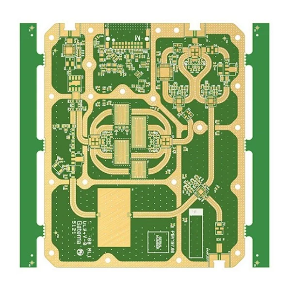
The rapid expansion of Electric Vehicle (EV) infrastructure relies heavily on robust connection standards, specifically the Combined Charging System (CCS). At the heart of every charging station and onboard vehicle interface lies the CCS Combo PCB. This circuit board is not merely a passive connector; it is a complex control center responsible for managing high-voltage power transfer, safety interlocks, and the critical communication handshake between the vehicle and the grid.
For engineers and procurement managers at APTPCB (APTPCB PCB Factory), understanding the nuances of this board is essential. Unlike a standard consumer electronics board, a CCS Combo PCB must withstand extreme thermal cycling, high voltages up to 1000V, and rigorous automotive reliability standards. This guide covers the entire lifecycle of these boards, from initial material selection to final validation, ensuring your EV charging projects meet global safety and performance benchmarks.
Key Takeaways
- Definition: A CCS Combo PCB manages the physical interface and communication protocol (ISO 15118) for DC fast charging and AC charging within a single footprint.
- Critical Metric: The Comparative Tracking Index (CTI) of the laminate is vital; it must typically exceed 600V to prevent arcing under high voltage.
- Thermal Management: Heavy copper (3oz+) and thermal vias are non-negotiable for DC fast charging variants to handle currents exceeding 200A.
- Signal Integrity: Impedance control is required for the Power Line Communication (PLC) lines to ensure the vehicle and charger "speak" correctly.
- Validation: Automated Optical Inspection (AOI) is insufficient; High Potential (Hi-Pot) testing is mandatory to verify isolation.
- Misconception: Not all CCS boards are the same; a Type 1 (US) PCB layout differs significantly from a Type 2 (EU) layout in pin configuration.
- Tip: Involve your manufacturer early to balance copper thickness with minimum trace spacing requirements.
What heavily on robust connection standards, specifically Combined Charging System (CCS) Combo PCB really means (scope & boundaries)
Building on the key takeaways, it is important to define exactly what falls under the scope of a CCS Combo PCB. The "Combo" in CCS stands for the combination of AC and DC charging pins in one inlet. Consequently, the PCB supporting this system must handle two distinct domains: the logic/communication domain and the high-power domain.
In the context of manufacturing, this term usually refers to two specific types of boards. First, it refers to the EVSE (Electric Vehicle Supply Equipment) Controller, which sits inside the charging station. This board interprets the pilot signals and manages the contactors. Second, it refers to the Inlet PCB located on the vehicle side or the connector gun, which physically routes the high-current pins to the battery management system or the AC-DC Converter PCB.
The complexity arises because these boards must integrate low-voltage communication signals (Control Pilot and Proximity Pilot) alongside high-voltage DC rails. This requires strict adherence to creepage and clearance rules defined by IEC 60664. Unlike a standard AC Charger PCB which only manages lower power levels, the CCS variant must survive the stress of DC fast charging, often reaching 350kW or more.
heavily on robust connection standards, specifically Combined Charging System (CCS) Combo PCB metrics that matter (how to evaluate quality)
Understanding the definition helps, but to manufacture a reliable board, you must quantify quality using specific metrics. High-voltage applications demand materials and tolerances that exceed standard IPC Class 2 requirements.
The following table outlines the critical parameters you must specify when ordering these boards from APTPCB.
| Metric | Why it matters | Typical range or influencing factors | How to measure |
|---|---|---|---|
| CTI (Comparative Tracking Index) | Prevents electrical breakdown (tracking) across the surface under voltage. | PLC 0 (≥600V) is standard for EV high-voltage circuits. | IEC 60112 test method. |
| Copper Weight | Determines current carrying capacity and thermal dissipation. | 3oz to 6oz (105µm - 210µm) for power paths; 1oz for logic. | Micro-section analysis. |
| Tg (Glass Transition Temp) | Ensures the board does not soften or delaminate during thermal stress. | High Tg (≥170°C) is recommended for automotive reliability. | DSC (Differential Scanning Calorimetry). |
| Dielectric Breakdown Voltage | Measures the insulation strength of the substrate material. | >40kV/mm is preferred to prevent internal arcing. | Hi-Pot testing (dielectric withstand). |
| Impedance Control | Essential for the PLC communication signal (Green PHY) stability. | 50Ω or 100Ω differential ±10%. | TDR (Time Domain Reflectometry). |
| Solder Mask Web | Prevents solder bridging between fine-pitch pins and high-voltage pads. | Min 4 mil (0.1mm); dependent on copper thickness. | AOI or visual inspection. |
| CAF Resistance | Prevents Conductive Anodic Filament growth over time in humid environments. | Must be Anti-CAF grade laminate. | Temperature-Humidity-Bias (THB) testing. |
How to choose heavily on robust connection standards, specifically Combined Charging System (CCS) Combo PCB: selection guidance by scenario (trade-offs)
Once you understand the metrics, the next step is selecting the right board architecture for your specific application. Not every charger needs a heavy copper board, and over-specifying drives up costs unnecessarily.
Here is how to choose the right CCS Combo PCB configuration based on six common deployment scenarios.
1. Home AC Wallbox (Level 2)
- Requirement: 7kW to 22kW AC charging.
- Recommendation: Standard FR4, Tg 150°C, 2oz copper.
- Trade-off: Lower cost, but limited thermal headroom. Not suitable for DC fast charging upgrades.
- Focus: Cost-efficiency and compact layout.
2. Public DC Fast Charger (50kW)
- Requirement: Moderate DC charging, often found in city centers.
- Recommendation: High Tg (170°C) FR4, 3oz copper, partial heavy copper technology.
- Trade-off: Higher cost than AC boards. Requires careful thermal simulation.
- Focus: Balancing thermal management with board size.
3. Ultra-Fast HPC Station (350kW - Liquid Cooled)
- Requirement: Extreme power delivery for highway charging.
- Recommendation: Heavy Copper PCB (4oz-6oz) or Metal Core PCB (MCPCB) for specific power modules.
- Trade-off: Very high manufacturing cost and longer lead times. Complex assembly.
- Focus: Maximum heat dissipation and current capacity.
4. Onboard Charger (OBC) Interface
- Requirement: The vehicle-side inlet PCB that connects to the battery.
- Recommendation: Automotive-grade materials (IATF 16949 compliant), Anti-CAF laminate.
- Trade-off: Strict validation requirements increase development time.
- Focus: Vibration resistance and long-term reliability (10+ years).
5. Portable EVSE (Emergency Charger)
- Requirement: Rugged, mobile charging unit.
- Recommendation: Rigid-Flex PCB to fit into compact, ergonomic handles.
- Trade-off: Higher unit price due to flex materials, but improves durability and packaging.
- Focus: Mechanical flexibility and shock resistance.
6. V2G (Vehicle-to-Grid) Bi-directional System
- Requirement: Power flows both to and from the vehicle.
- Recommendation: Complex multilayer stackup (6-8 layers) to handle complex logic and power switching.
- Trade-off: Signal integrity becomes challenging due to switching noise.
- Focus: EMI shielding and precise impedance control.
heavily on robust connection standards, specifically Combined Charging System (CCS) Combo PCB implementation checkpoints (design to manufacturing)

After selecting the right approach, you move into the execution phase. Manufacturing a CCS Combo PCB requires a disciplined process to avoid costly scrap events.
Use this checklist to guide your project from design files to the final product.
- Schematic Validation: Verify that the Control Pilot (CP) and Proximity Pilot (PP) circuits are isolated from the high-voltage DC lines.
- Material Selection: Confirm the laminate datasheet explicitly states CTI ≥ 600V and is Anti-CAF. Do not rely on generic "FR4" specifications.
- Stackup Design: For high currents, place power planes on internal layers with sufficient copper weight, but ensure prepreg thickness is adequate for dielectric isolation.
- Clearance Verification: Run a DFM check specifically for high voltage. Ensure creepage distances meet IEC 60664 standards (often >8mm for certain voltage classes).
- Drilling Strategy: If using heavy copper, ensure the drill bit size accounts for the thicker plating required in the barrel. Aspect ratio should be kept conservative (below 8:1).
- Etching Compensation: Heavy copper requires significant etch compensation. Design traces slightly wider in the CAD file to account for the material removed during etching.
- Solder Mask Application: Use multiple coats of solder mask or specific high-voltage plug-via inks to ensure no voids exist that could lead to arcing.
- Surface Finish: Electroless Nickel Immersion Gold (ENIG) is preferred for flat pads and corrosion resistance, especially for the communication pins.
- Electrical Testing (E-Test): Specify a higher voltage for the netlist test than standard boards. Standard is often 100V; for CCS, request 250V or higher if possible for isolation testing.
- Final Quality Audit: Perform a 100% visual inspection for copper burrs or potential shorts, which are catastrophic in high-voltage environments.
heavily on robust connection standards, specifically Combined Charging System (CCS) Combo PCB common mistakes (and the correct approach)
Even with a checklist, errors can occur. The unique demands of the CCS Combo PCB often trip up designers accustomed to low-voltage electronics.
1. Ignoring Creepage and Clearance
- Mistake: Using standard 5-mil spacing rules on a board carrying 400V+.
- Correction: Use a calculator based on IEC standards. You may need slots (routing out PCB material) between high-voltage pads to effectively increase the creepage distance without increasing board size.
2. Underestimating Thermal Rise
- Mistake: Assuming a standard trace width calculator applies to an enclosed, non-ventilated charging gun.
- Correction: Use High Thermal PCB design principles. Simulate the temperature rise assuming the worst-case ambient temperature (often 50°C inside a charging station).
3. Poor PLC Signal Routing
- Mistake: Routing the communication lines (CP/PP) parallel to the high-voltage DC switching lines.
- Correction: Route differential pairs away from power planes. Use ground shielding or guard traces to protect the integrity of the communication handshake.
4. Wrong Copper Thickness Specification
- Mistake: Specifying 1oz copper and relying on solder to carry the current.
- Correction: Specify 3oz or 4oz base copper. Solder has much higher resistance than copper and should not be the primary current carrier for high-amperage paths.
5. Neglecting Environmental Protection
- Mistake: Leaving the PCB exposed without conformal coating.
- Correction: EV chargers are outdoor equipment. Apply a silicone or acrylic conformal coating to protect against humidity and dust.
6. Inadequate Via Capacity
- Mistake: Using a single standard via for a 10A current path.
- Correction: Use via arrays (stitching) to transition high currents between layers. Calculate the current capacity per via and add a 50% safety margin.
heavily on robust connection standards, specifically Combined Charging System (CCS) Combo PCB FAQ (cost, lead time, materials, testing, acceptance criteria)
Q: What is the typical cost difference between a standard PCB and a CCS Combo PCB? A: A CCS board typically costs 30-50% more than a standard board of the same size. This is due to the requirement for high-CTI materials, heavy copper (which consumes more etchant and plating time), and stricter testing protocols.
Q: How does the lead time compare for heavy copper CCS boards? A: Standard PCBs might take 3-5 days. Heavy copper boards (>3oz) often require 8-12 days because the lamination and plating cycles are longer and require slower, more precise etching processes.
Q: Can I use standard FR4 for a CCS Combo PCB? A: For the logic section, yes. However, for the high-voltage sections, standard FR4 often has a CTI of 175V-250V. You must specify "High CTI" (PLC 0) FR4 to meet safety standards for 600V+ applications.
Q: What are the acceptance criteria for high-voltage isolation testing? A: The board must pass a Hi-Pot test where a high voltage (often 1000VDC +) is applied between isolated nets. The acceptance criterion is typically leakage current below a specific threshold (e.g., <1mA) with no breakdown or flashover.
Q: Do I need specific surface finishes for the connector pads? A: Yes. Hard Gold is often recommended for the actual connector fingers if they are part of the PCB (edge connector style) due to its wear resistance. For component pads, ENIG is preferred for flatness and reliability.
Q: How do I handle the heat from the AC-DC Converter PCB section? A: If your CCS system includes the power conversion stage, consider using a metal core or embedding copper coins into the PCB to physically conduct heat away from MOSFETs or IGBTs to the chassis.
Q: What data is needed for a DFM review of a CCS board? A: Beyond Gerber files, you must provide the netlist, a stackup drawing specifying dielectric voltages, current requirements per net, and any specific isolation zones that need routing slots.
Q: Is UL certification required for the bare PCB? A: Yes, the bare board manufacturer (like APTPCB) should hold a UL 94 V-0 flammability rating. The final assembly will likely need system-level certification (UL 2202 or similar), which relies on the PCB's underlying certification.
Resources for heavily on robust connection standards, specifically Combined Charging System (CCS) Combo PCB (related pages and tools)
To further assist in your design and procurement process, we have curated a list of relevant resources and capabilities available at APTPCB.
- For High Power Needs: Explore our Automotive Electronics PCB capabilities, which are tailored for the rigorous demands of EV infrastructure.
- For Assembly Services: If you need the components populated, our Turnkey Assembly service handles component sourcing and soldering, including heavy components like relays and connectors.
- Design Guidelines: Review our DFM suggestions for Heavy Copper PCB to ensure your high-current traces are manufacturable.
heavily on robust connection standards, specifically Combined Charging System (CCS) Combo PCB glossary (key terms)
| Term | Definition |
|---|---|
| CCS (Combined Charging System) | A standard for charging electric vehicles that uses the Combo 1 or Combo 2 connectors to provide power at up to 350 kilowatts. |
| EVSE (Electric Vehicle Supply Equipment) | The infrastructure that supplies electric energy for the recharging of electric vehicles (the charging station). |
| CP (Control Pilot) | A communication line in the charging cable used to signal the charging level between the car and the charger. |
| PP (Proximity Pilot) | A safety line that ensures the connector is fully inserted and prevents the car from driving away while connected. |
| PLC (Power Line Communication) | A communication method where data is sent over the existing power cables; used in CCS for the digital handshake. |
| BMS (Battery Management System) | The system inside the EV that manages the battery pack; the CCS PCB communicates with this system. |
| OBC (Onboard Charger) | The device inside the vehicle that converts AC power from the grid to DC power for the battery. |
| Creepage | The shortest distance between two conductive parts along the surface of a solid insulating material. |
| Clearance | The shortest distance between two conductive parts through the air. |
| CTI (Comparative Tracking Index) | A measure of the electrical breakdown (tracking) properties of an insulating material. |
| Heavy Copper | PCB manufacturing technology using ≥3oz of copper to handle high current loads. |
| ISO 15118 | The international standard defining the vehicle-to-grid communication interface for charging. |
Conclusion (next steps)
The CCS Combo PCB is a critical enabler of the electric mobility revolution. It bridges the gap between the power grid and the vehicle, requiring a delicate balance of high-power handling and precise communication capabilities. Whether you are designing a Level 2 home charger or a Level 3 DC fast charging station, the success of your product hinges on selecting the right materials, adhering to strict design rules, and partnering with a capable manufacturer.
At APTPCB, we specialize in the complexities of high-voltage and automotive-grade PCBs. To move your project forward, we recommend preparing your data for a comprehensive DFM review.
When requesting a quote, please provide:
- Gerber Files: RS-274X format.
- Stackup Details: Specifically mentioning CTI requirements and copper weights.
- Fabrication Drawing: Highlighting critical creepage zones and slot requirements.
- Test Requirements: Voltage levels for Hi-Pot testing.
By addressing these details early, you ensure a smooth transition from prototype to mass production, delivering a safe and reliable charging experience for EV users worldwide.