Key Takeaways
- Definition: A Central Station PCB acts as the data aggregation and processing hub for networked monitoring systems, primarily in medical (patient monitoring) and industrial control environments.
- Safety Standards: Compliance with IEC 60601-1 is non-negotiable; understanding the difference between 2 MOPP PCB (Patient Protection) and 2 MOOP PCB (Operator Protection) is critical for isolation design.
- Signal Integrity: These boards often function as high-speed servers, requiring controlled impedance and low-loss materials to handle real-time data streams without latency.
- Reliability: Unlike consumer electronics, these boards require IPC Class 3 manufacturing standards to ensure 24/7 continuous operation.
- Validation: Electrical testing must go beyond basic connectivity to include Hi-Pot testing and specific thermal stress analysis.
- Manufacturing Partner: Early engagement with a capable manufacturer like APTPCB (APTPCB PCB Factory) ensures design intent matches production capabilities.
What Central Station PCB really means (scope & boundaries)
Before diving into technical specifications, it is essential to define the operational scope of a Central Station PCB to distinguish it from standard motherboards.
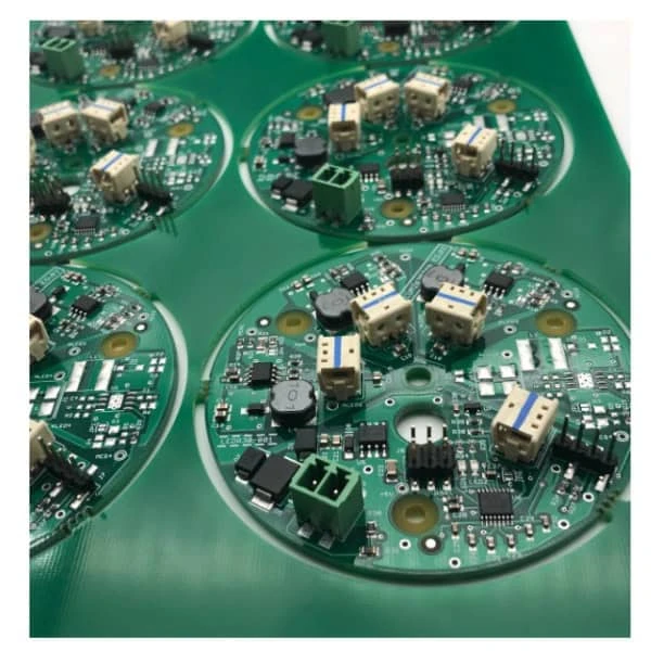
A Central Station PCB is the hardware foundation of a Central Nursing Station (CNS) or a Centralized Control Room. In a hospital setting, this board processes vital signs from multiple bedside monitors simultaneously. It is not merely a computer; it is a safety-critical device that aggregates, analyzes, and displays real-time data. If this board fails, the entire monitoring network goes blind.
The scope of these PCBs extends beyond simple connectivity. They must handle:
- High-Speed Data Processing: Aggregating video, waveforms, and telemetry data.
- Power Management: Distributing stable power to sub-modules while isolating high-voltage mains from sensitive logic.
- Environmental Resilience: Withstanding continuous heat generation and potential exposure to cleaning chemicals.
In industrial contexts, a similar architecture applies. However, the focus shifts from patient safety to operator safety and noise immunity. Whether for a hospital or a factory, the defining characteristic is "zero downtime."
Central Station PCB metrics that matter (how to evaluate quality)
Once you understand the operational scope, you must quantify quality using specific engineering metrics rather than vague promises.
The following table outlines the critical performance indicators for a high-reliability Central Station PCB.
| Metric | Why it matters | Typical Range / Factor | How to Measure |
|---|---|---|---|
| Dielectric Strength | Ensures isolation between high-voltage power and low-voltage logic (Safety). | > 1.5 kV (AC) or > 4.0 kV depending on MOPP/MOOP rating. | Hi-Pot (High Potential) Testing. |
| Differential Impedance | Prevents data corruption in high-speed interfaces (Ethernet, HDMI, LVDS). | 90Ω or 100Ω ±10% (or tighter ±5%). | TDR (Time Domain Reflectometry). |
| Tg (Glass Transition Temp) | Determines the board's ability to withstand heat without expanding excessively. | High Tg (> 170°C) is standard for central stations. | TMA (Thermomechanical Analysis). |
| CAF Resistance | Prevents internal short circuits caused by electrochemical migration over time. | Must pass 500-1000 hours at high humidity/voltage. | Temperature-Humidity-Bias (THB) Test. |
| Copper Plating Thickness | Ensures barrel integrity in vias during thermal cycling. | IPC Class 3 requires average 25µm (1 mil). | Cross-section analysis (Microsection). |
| CTE (z-axis) | Prevents via cracking during soldering and operation. | < 3.5% expansion (50°C to 260°C). | TMA. |
How to choose Central Station PCB: selection guidance by scenario (trade-offs)
Metrics provide the data, but the specific application context dictates which trade-offs are acceptable during the selection process.
Different environments impose different constraints. Below are common scenarios and how to choose the right PCB architecture.
1. ICU Central Monitoring (Patient Safety Critical)
- Requirement: The system connects indirectly to patient sensors.
- Choice: You must select a 2 MOPP PCB design strategy.
- Trade-off: Requires larger creepage and clearance distances (e.g., 8mm for mains voltage). This reduces available board space for components, forcing a move to higher layer counts or HDI technology.
2. Industrial Control Hub (Operator Safety)
- Requirement: The system controls high-voltage machinery but does not touch patients.
- Choice: A 2 MOOP PCB design is sufficient.
- Trade-off: Isolation distances are slightly more lenient than MOPP, allowing for denser layouts. However, you must prioritize EMI shielding to reject factory floor noise.
3. Telemetry Server (High-Speed Data Focus)
- Requirement: Processing massive amounts of wireless data from portable packs.
- Choice: Focus on High Speed PCB materials (Low Dk/Df).
- Trade-off: Materials like Rogers or Megtron are significantly more expensive than FR4. You might use a hybrid stackup (FR4 + High-Speed material) to balance cost.
4. Compact Nursing Station (Space Constrained)
- Requirement: Fits into a small, wall-mounted enclosure.
- Choice: HDI (High Density Interconnect) with blind/buried vias.
- Trade-off: Higher manufacturing cost and complexity. Thermal management becomes harder because heat is concentrated in a smaller area.
5. Legacy Retrofit (Compatibility Focus)
- Requirement: Must fit into an existing rack or casing from 10 years ago.
- Choice: Standard Rigid PCB with thick copper for power rails.
- Trade-off: Limited by the physical dimensions of the old enclosure. You may need to use rigid-flex to route signals around awkward mechanical obstacles.
6. AI-Diagnostic Hub (High Thermal Load)
- Requirement: On-board GPU for real-time arrhythmia analysis.
- Choice: Metal Core PCB (MCPCB) or heavy copper with thermal vias.
- Trade-off: Excellent cooling but limited routing layers compared to standard FR4. Often requires a separate module for the processing unit.
Central Station PCB implementation checkpoints (design to manufacturing)

Selecting the right approach is useless without precise execution during the design and fabrication phases.
To ensure your Central Station PCB functions correctly on the first run, follow this checkpoint list.
1. Schematic Capture & Isolation Logic
Define your isolation barriers early. Clearly mark the "Primary" (Mains) and "Secondary" (Patient/Operator) sides. If your schematic does not visually separate these grounds, the layout engineer will likely make a mistake.
2. Stackup Design
Do not leave the stackup to the last minute. For high-speed central stations, define the layer count based on impedance requirements. Consult APTPCB during this phase to verify material availability.
3. Material Selection
Choose materials that resist Conductive Anodic Filament (CAF) growth. Central stations run 24/7, often in humid environments. Standard FR4 may not suffice; specify "CAF-Resistant High-Tg FR4."
4. Layout: Creepage and Clearance
This is the most common failure point for 2 MOPP PCB designs.
- Clearance: The shortest path through air.
- Creepage: The shortest path along the surface.
- Action: Set CAD rules to flag any violation of IEC 60601 spacing (e.g., 8mm for 2 MOPP at 250V). Slots can be routed into the PCB to increase creepage distance without moving components.
5. Thermal Management
Central stations are often fanless to reduce noise and dust.
- Recommendation: Use thermal vias under hot components (CPU, FPGA).
- Risk: If vias are not tented or plugged correctly, solder can wick away, leading to poor thermal contact.
6. Solder Mask & Legend
Ensure the solder mask dam between pads is sufficient (typically 4 mil minimum). For medical boards, avoid placing white legend ink over pads, as this compromises solder joint reliability.
7. Surface Finish
Select ENIG (Electroless Nickel Immersion Gold) or ENEPIG. These finishes provide a flat surface for fine-pitch components (BGAs) and offer excellent corrosion resistance compared to HASL.
8. Final Validation (DFM Review)
Before ordering, run a comprehensive DFM check. Look for acid traps, slivers, and unconnected vias. A Medical PCB requires stricter tolerances than consumer boards.
Central Station PCB common mistakes (and the correct approach)
Even with a solid plan, specific errors frequently occur in the development of Central Station PCBs.
1. Confusing MOOP and MOPP
- Mistake: Applying 2 MOOP PCB standards (Operator Protection) to a device that connects to a patient.
- Correction: Always assume the strictest standard (MOPP) if there is any chance of patient contact via sensors or cables. 2 MOPP requires double the isolation of basic insulation.
2. Neglecting the "Y-Cap" Ground Leakage
- Mistake: Using standard EMI filter capacitors that allow too much leakage current to ground.
- Correction: In medical central stations, leakage current limits are extremely low (often < 100µA). Use medical-grade components and minimize parasitic capacitance in the PCB layout.
3. Poor Reference Plane Management
- Mistake: Routing high-speed traces over a split in the ground plane (often caused by isolation gaps).
- Correction: Never cross a split plane with a high-speed signal. It creates a massive return loop, causing EMI failures. Use bridge capacitors or optocouplers to cross isolation barriers.
4. Ignoring Mechanical Stress on Connectors
- Mistake: Placing heavy I/O connectors (Ethernet, Power) without mechanical reinforcement.
- Correction: Central stations are plugged and unplugged frequently. Add through-hole mounting tabs or additional fiducials for mechanical strength, even if the signal pins are SMT.
5. Underestimating Thermal Aging
- Mistake: Designing for "Room Temperature" specs.
- Correction: These boards run hot inside enclosures. Ensure the laminate's MOT (Maximum Operating Temperature) is well above the internal ambient temperature.
6. Skipping the First Article Inspection (FAI)
- Mistake: Going straight to mass production.
- Correction: Always perform a First Article Inspection to validate the physical dimensions and electrical performance before full-scale fabrication.
Central Station PCB FAQ (cost, lead time, Design for Manufacturability (DFM) files, stackup, impedance, Dk/Df)
Addressing specific errors often leads to broader questions about standards and lifecycle.
Q: What is the difference between 1 MOPP and 2 MOPP? A: MOPP stands for "Means of Patient Protection." 1 MOPP provides basic insulation. 2 MOPP provides double insulation and is required for devices where electrical failure could harm the patient. 2 MOPP requires stricter creepage (8mm) and dielectric strength (4000V).
Q: Can I use standard FR4 for a Central Station PCB? A: It depends on the speed and thermal load. For basic monitoring, High-Tg FR4 is acceptable. For high-speed telemetry servers, low-loss materials are recommended to preserve signal integrity.
Q: How do I ensure my PCB meets IEC 60601-1? A: You must design the isolation barriers (creepage/clearance) into the layout and select materials with the correct CTI (Comparative Tracking Index). The PCB manufacturer must also provide UL certification for flammability (typically 94V-0).
Q: What is the typical lifespan of a Central Station PCB? A: Unlike consumer electronics (3-5 years), medical and industrial central stations are designed for 7-10+ years of service. This requires high-reliability materials and conservative design rules.
Q: Does APTPCB handle the assembly (PCBA) for these boards? A: Yes, full turnkey services including component sourcing, SMT assembly, and functional testing are available to ensure the entire system meets quality standards.
Q: Why is impedance control critical for these boards? A: Central stations aggregate data via Ethernet, USB, or HDMI. If the impedance mismatches, data packets are lost (jitter/reflection), causing the monitoring screen to freeze or lag—a critical failure in medical contexts.
Q: What surface finish is best for long-term reliability? A: ENIG is the industry standard for high-reliability boards. It prevents oxidation and provides a flat surface for fine-pitch components.
Q: How does "2 MOOP PCB" differ in design? A: 2 MOOP PCB focuses on protecting the operator. The isolation distances are slightly smaller than MOPP, but the design must still prevent shock hazards to staff touching the console.
Central Station PCB glossary (key terms)
| Term | Definition |
|---|---|
| MOPP | Means of Patient Protection. A safety standard defined by IEC 60601-1. |
| MOOP | Means of Operator Protection. Similar to MOPP but with slightly different voltage/spacing requirements. |
| Creepage | The shortest distance between two conductive parts along the surface of the insulation. |
| Clearance | The shortest distance between two conductive parts through the air. |
| CTI | Comparative Tracking Index. Measures the electrical breakdown (tracking) properties of the insulating material. |
| HDI | High Density Interconnect. PCB technology using microvias to increase circuit density. |
| Blind Via | A via connecting an outer layer to an inner layer, not visible from the other side. |
| Buried Via | A via connecting inner layers only, not visible from the outside. |
| EMI | Electromagnetic Interference. Noise that disrupts signal quality. |
| IPC Class 3 | The highest manufacturing standard for PCBs, used for life-support and aerospace systems. |
| Stackup | The arrangement of copper layers and insulating material in a PCB. |
| Gerber Files | The standard file format used to send PCB designs to manufacturing. |
Conclusion (next steps)
The Central Station PCB is the silent guardian of modern monitoring networks. Whether you are designing a 2 MOPP PCB for an ICU or a 2 MOOP PCB for an industrial control room, the margin for error is non-existent. Success lies in balancing rigorous safety standards (IEC 60601) with high-speed performance and thermal reliability.
To move from concept to production, you need to provide your manufacturer with a complete data package. This includes:
- Gerber Files: RS-274X format preferred.
- Fabrication Drawing: Specifying IPC Class 3, material requirements (Tg, CTI), and surface finish.
- Stackup Diagram: Detailing layer order and impedance constraints.
- Netlist: For electrical validation.
At APTPCB, we specialize in high-reliability manufacturing for medical and industrial sectors. If you are ready to validate your design or need a Quote for your next project, contact our engineering team today. We ensure your central station is built to save lives and secure data.