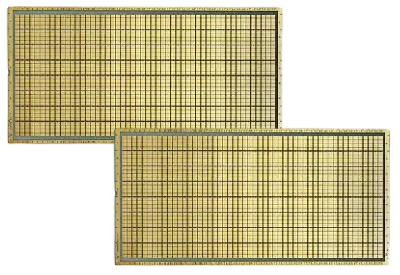
Chemical Sensor PCB technology sits at the intersection of electronics and chemistry. These boards do not just carry signals; they often interact directly with the environment to detect gases, liquids, or biological markers. Designing them requires a shift in mindset from standard digital logic to sensitive analog precision and material durability.
At APTPCB (APTPCB PCB Factory), we see an increasing demand for sensors that can withstand harsh industrial chemicals or provide medical-grade accuracy. This guide covers the entire lifecycle of a Chemical Sensor PCB, from the initial definition to the final production validation.
Key Takeaways
- Definition: A Chemical Sensor PCB acts as both the physical support and the electrical interface for sensing elements, often requiring specialized substrates like ceramic or Teflon.
- Critical Metric: Surface insulation resistance (SIR) is more vital than standard impedance, as leakage currents can mimic sensor signals.
- Material Choice: Standard FR4 absorbs moisture; ceramic or polyimide is often required for stability in chemical environments.
- Misconception: Many designers believe standard solder mask is sufficient protection; however, chemical sensors often require specialized passivation or open windows for analytes.
- Tip: Use guard rings on the PCB layout to protect high-impedance sensor lines from leakage currents.
- Validation: Testing must include environmental exposure cycles, not just electrical continuity.
- Manufacturing: Cleanliness is paramount; ionic residues from manufacturing can destroy sensor accuracy.
What Chemical Sensor PCB really means (scope & boundaries)
Understanding the core definition helps clarify why these boards differ from standard consumer electronics. A Chemical Sensor PCB is a printed circuit board specifically engineered to host or integrate a transducer that converts a chemical reaction into an electrical signal.
The Scope
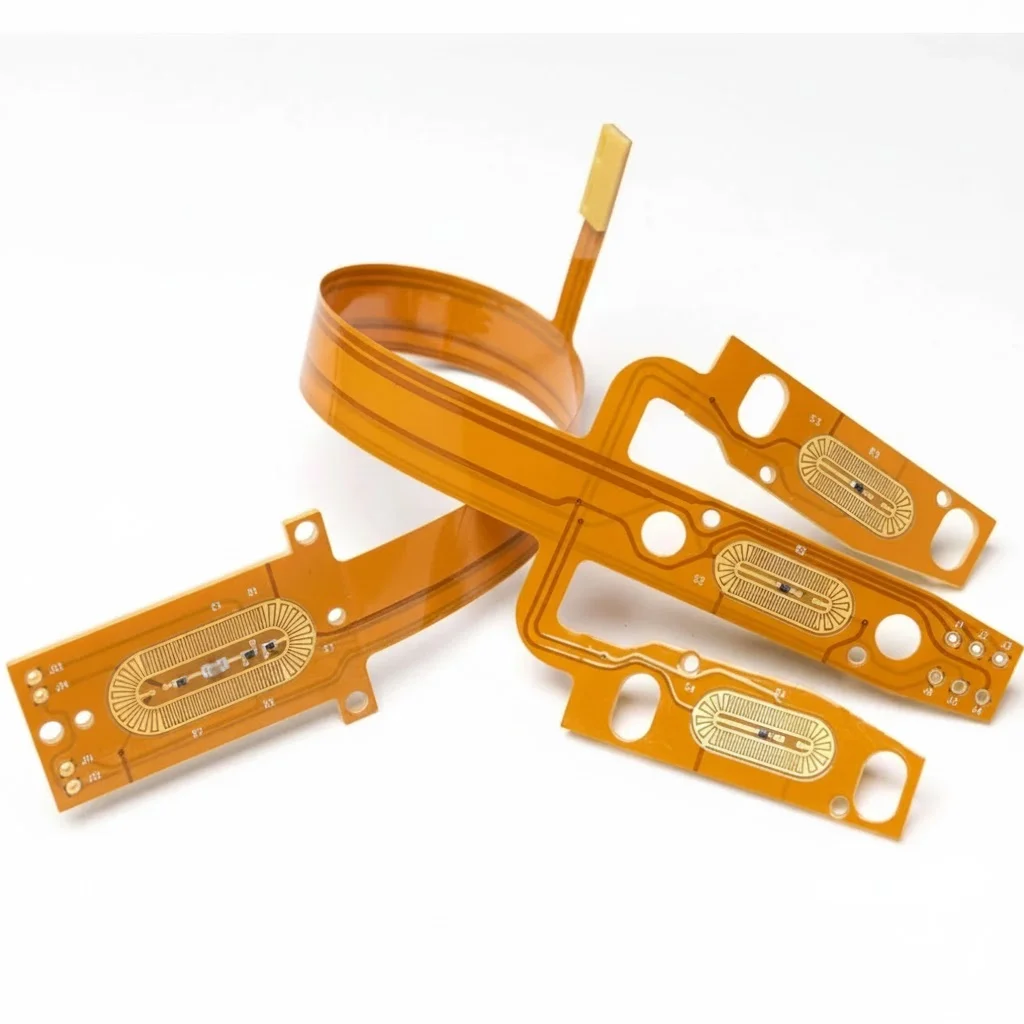
The term covers two distinct architectures. First, the PCB may serve as the substrate for the sensor itself. In this case, the copper traces (often plated with gold or platinum) form the electrodes—such as Interdigitated Electrodes (IDEs)—that directly contact the chemical analyte. Second, the PCB may act as the readout interface, where a separate chemical sensor component is mounted to the board. This guide focuses heavily on the first type, as it presents the most manufacturing challenges, but the principles apply to both.
The Boundaries
This technology is distinct from standard IoT boards. A standard board focuses on processing speed and power distribution. A Chemical Sensor PCB focuses on signal integrity at the picoampere level and material inertness. If the PCB material reacts with the target chemical, the sensor fails. Therefore, the boundary of this technology is defined by material science compatibility rather than just circuit density.
Chemical Sensor PCB metrics that matter (how to evaluate quality)
Once the scope is defined, you must establish quantifiable metrics to ensure the sensor performs as intended. Unlike digital boards where "pass/fail" is binary, chemical sensors operate on a spectrum of sensitivity.
| Metric | Why it matters | Typical range / Factors | How to measure |
|---|---|---|---|
| Leakage Current | High-impedance sensors generate tiny currents. Board leakage creates false positives. | < 100 fA (femtoamperes) for high precision. | Electrometer with guarded probes. |
| Surface Roughness | Affects the adhesion of sensing layers (e.g., polymers or nanomaterials) applied to electrodes. | Ra < 0.5 µm for thin films. | Profilometer or Atomic Force Microscopy. |
| Thermal Stability | Chemical reaction rates change with temperature. The PCB must not warp or drift thermally. | CTE < 7 ppm/°C (Ceramic) vs 14-17 ppm/°C (FR4). | TMA (Thermomechanical Analysis). |
| Chemical Resistance | The substrate must not swell, dissolve, or outgas when exposed to the analyte. | Material specific (e.g., Acetone resistance, Acid resistance). | Immersion testing (24h - 7 days). |
| Electrode Flatness | Critical for uniform sensing area and consistent current density. | Planarity within ±10%. | 3D Optical Inspection. |
| Ionic Cleanliness | Residues from flux or plating cause drift and corrosion. | < 0.5 µg/cm² NaCl equivalent. | Ion Chromatography (Rose Test). |
How to choose Chemical Sensor PCB: selection guidance by scenario (trade-offs)
Metrics provide the data, but the application environment dictates the design choices. Below are common scenarios and how to choose the right Chemical Sensor PCB configuration for each.
Scenario 1: Harsh Industrial Gas Detection
- Environment: High temperature, corrosive gases (Chlorine, Ammonia).
- Recommendation: Ceramic PCB (Alumina or Aluminum Nitride).
- Trade-off: Higher cost and brittle mechanical properties, but offers unmatched chemical inertness and thermal stability.
Scenario 2: Wearable Sweat or Glucose Monitoring
- Environment: Skin contact, bending, moisture.
- Recommendation: Rigid-Flex PCB or Polyimide Flex.
- Trade-off: Complex manufacturing process. Requires biocompatible coverlays instead of standard solder masks.
Scenario 3: Disposable Medical Test Strips
- Environment: Single-use, room temperature, aqueous solutions.
- Recommendation: High-Tg FR4 or Paper-based electronics with Carbon/Silver ink printing.
- Trade-off: Lower sensitivity and durability, but extremely low cost for mass volume.
Scenario 4: High-Precision Lab Analytics
- Environment: Controlled lab setting, extremely low detection limits.
- Recommendation: PTFE (Teflon) or Rogers substrates.
- Trade-off: Difficult to plate and process, but provides the lowest dielectric absorption and leakage current.
Scenario 5: Automotive Exhaust Sensing
- Environment: Extreme heat (>300°C), vibration, soot.
- Recommendation: Thick-film Ceramic or Metal Core PCB (with dielectric isolation).
- Trade-off: Heavy and requires specialized mounting to manage vibration stress on ceramic parts.
Scenario 6: Underwater/Marine Quality Monitoring
- Environment: High pressure, saline corrosion, bio-fouling.
- Recommendation: FR4 with specialized Conformal Coating (Parylene) and potting.
- Trade-off: Rework is impossible after potting. The sensor window must be carefully masked during coating.
Chemical Sensor PCB implementation checkpoints (design to manufacturing)

After selecting the right scenario, the focus shifts to execution. APTPCB recommends following these specific checkpoints to move from a design file to a functional product.
Material Verification:
- Recommendation: Confirm the substrate datasheet for chemical compatibility with your specific analyte.
- Risk: FR4 epoxy swelling in certain solvents.
- Acceptance: Material certification review.
Electrode Layout Design:
- Recommendation: Use rounded corners on interdigitated electrodes to reduce electric field concentration.
- Risk: Arcing or non-uniform sensing fields.
- Acceptance: DRC (Design Rule Check) for spacing < 4 mil if applicable.
Guard Ring Implementation:
- Recommendation: Place driven guard rings around high-impedance sensor traces.
- Risk: Signal drift due to surface leakage currents.
- Acceptance: Electrical simulation or schematic review.
Surface Finish Selection:
- Recommendation: Use ENEPIG or Hard Gold. Avoid HASL (too rough) or OSP (organic contamination).
- Risk: Oxidation of contacts affecting sensor baseline.
- Acceptance: Surface Finish thickness measurement (X-Ray).
Solder Mask Definition:
- Recommendation: Define "Solder Mask Defined" (SMD) or "Non-Solder Mask Defined" (NSMD) pads explicitly based on sensor exposure needs.
- Risk: Mask encroachment covering the active sensing area.
- Acceptance: Visual inspection of the sensor window.
Panelization Strategy:
- Recommendation: Ensure V-cuts or break-away tabs do not stress the sensor area.
- Risk: Micro-cracks in ceramic or sensor delamination.
- Acceptance: Stress analysis or prototype trial.
Assembly Flux Selection:
- Recommendation: Use "No-Clean" flux, but clean it anyway. Or use water-soluble flux with aggressive washing.
- Risk: Active flux residues reacting with the sensor chemistry.
- Acceptance: Ionic contamination testing.
Encapsulation/Potting:
- Recommendation: Use low-stress potting compounds that cure without significant shrinkage.
- Risk: Piezoresistive effect shifting sensor readings due to pressure.
- Acceptance: Thermal cycling test.
Final Cleaning:
- Recommendation: Plasma cleaning before sensor functionalization.
- Risk: Hydrophobic contaminants preventing sensor layer adhesion.
- Acceptance: Water contact angle measurement.
Functional Testing:
- Recommendation: Test a subset of boards with a calibration gas/liquid.
- Risk: Batch-to-batch variation in sensitivity.
- Acceptance: Statistical Process Control (SPC) on baseline voltage.
Chemical Sensor PCB common mistakes (and the correct approach)
Even with a solid plan, specific pitfalls often trap designers. Avoiding these ensures a smoother production run.
Mistake: Ignoring the Galvanic Effect.
- Context: Using dissimilar metals (e.g., Gold and Tin) in a humid environment.
- Result: Rapid corrosion at the interface, destroying the connection.
- Correction: Use compatible metal systems or encapsulate the junction completely.
Mistake: Relying on Standard FR4 for Everything.
- Context: Using FR4 for sensors detecting moisture or humidity.
- Result: The PCB absorbs water, changing its dielectric constant and causing baseline drift.
- Correction: Switch to hydrophobic substrates like Rogers or Liquid Crystal Polymer (LCP).
Mistake: Overlooking Thermal EMF.
- Context: Creating temperature gradients across the PCB layout.
- Result: Thermocouple effects generate voltage offsets in microvolt-level sensors.
- Correction: Layout symmetric traces and keep heat-generating components away from the analog front end.
Mistake: Incomplete Flux Removal.
- Context: Assuming standard washing is enough for electrochemical sensors.
- Result: Residual ions create a battery effect, generating noise.
- Correction: Specify "Medical Grade" or "Sensor Grade" cleaning protocols in the fabrication notes.
Mistake: Poor Masking during Conformal Coating.
- Context: Spraying coating over the entire board.
- Result: The active sensor area is blocked and cannot detect the chemical.
- Correction: Design physical masking fixtures or use selective coating robots.
Mistake: Underestimating Trace Resistance.
- Context: Using thin, long traces for heater elements on the sensor.
- Result: Voltage drop causes the heater to run cooler than intended, affecting sensor sensitivity.
- Correction: Use wide traces or heavy copper for heater lines; use Kelvin connections for measurement.
Chemical Sensor PCB FAQ (cost, lead time, materials, testing, acceptance criteria)
Q: How does the cost of a Chemical Sensor PCB compare to a standard PCB? A: They are typically 30-50% more expensive due to specialized materials (Ceramic/Teflon), strict cleanliness requirements, and hard gold plating.
Q: What is the typical lead time for these boards? A: Standard FR4 sensors take 5-7 days. Ceramic or exotic material sensors often require 15-20 days due to material procurement and specialized firing/curing processes.
Q: Can I use standard HASL finish for chemical sensors? A: Generally, no. HASL is uneven and oxidizes. ENIG (Electroless Nickel Immersion Gold) or ENEPIG is preferred for flat, corrosion-resistant electrodes.
Q: How do you test the chemical resistance of the PCB? A: We perform immersion testing where the PCB is soaked in the target chemical (or a simulant) for a set period, followed by visual inspection for delamination and electrical testing for leakage.
Q: What are the acceptance criteria for visual inspection? A: For the sensing area, we follow IPC-6012 Class 3 standards or higher. No scratches, pits, or nodules are allowed on the electrode surfaces, as these alter the active surface area.
Q: Why is "Low CTE" important for chemical sensors? A: Many chemical sensors operate at elevated temperatures. If the PCB expands too much (High CTE), it can crack the sensing element or cause delamination of the thin-film electrodes.
Q: Can APTPCB manufacture PCBs with integrated microfluidic channels? A: Yes, we can produce multi-layer structures with milled channels or use specific bonding techniques to create cavities for fluid flow.
Q: What is the best material for high-impedance pH sensors? A: Teflon (PTFE) or high-quality Ceramic is best because they have extremely high surface insulation resistance, preventing leakage currents that would distort the pH reading.
Q: How do you handle the "drift" issue in PCB-based sensors? A: Drift is often caused by aging materials or contamination. We mitigate this by using high-stability substrates and ensuring rigorous ionic cleaning before shipping.
Q: Do you offer design services for the electrode geometry? A: While we are primarily a manufacturer, our DFM engineers can optimize your existing electrode design for manufacturability, ensuring trace widths and gaps are within reproducible limits.
Chemical Sensor PCB glossary (key terms)
| Term | Definition |
|---|---|
| Analyte | The chemical substance that the sensor is designed to detect or measure. |
| Interdigitated Electrodes (IDE) | A finger-like pattern of electrodes used to maximize the sensing surface area on a PCB. |
| Potentiostat | The electronic hardware (often integrated on the PCB) that controls the voltage and measures current in electrochemical sensors. |
| Passivation | A protective layer applied to the PCB to prevent corrosion in non-sensing areas. |
| Cross-sensitivity | When a sensor reacts to a chemical other than the target analyte (e.g., a CO sensor reacting to Hydrogen). |
| Drift | The gradual change in sensor output over time, independent of the analyte concentration. |
| Hysteresis | The difference in sensor output when approaching a value from a lower concentration versus a higher concentration. |
| Guard Ring | A copper trace surrounding a sensitive signal, driven to the same voltage to prevent leakage current. |
| Femtoampere (fA) | A unit of current ($10^{-15}$ Amperes). Chemical sensors often operate in this ultra-low range. |
| Substrate | The base material of the PCB (FR4, Ceramic, Polyimide) which provides mechanical support. |
| Microfluidics | The technology of manipulating small amounts of fluids, often integrated into the PCB structure. |
| Functionalization | The process of coating the PCB electrodes with a specific chemical layer to make them sensitive to the target analyte. |
Conclusion (next steps)
Successfully deploying a Chemical Sensor PCB requires balancing electrochemical performance with mechanical robustness. Whether you are building a disposable medical strip or a long-life industrial gas detector, the choice of substrate, surface finish, and cleanliness protocol will define your product's accuracy.
When you are ready to move to production, APTPCB is equipped to handle the stringent requirements of sensor fabrication. To get an accurate DFM review and quote, please provide:
- Gerber Files: Including specific layers for carbon ink, peelable masks, or special plating.
- Stackup Details: Specifying material types (e.g., Rogers 4003, Alumina Ceramic).
- Surface Finish: Thickness requirements for Gold or Platinum plating.
- Test Requirements: Specific leakage current limits or ionic cleanliness standards.
- Environmental Specs: The chemicals and temperatures the board must withstand.
Precision manufacturing ensures your sensor detects the signal, not the noise.