Key Takeaways
- Definition: Clarification PCB refers to specialized circuit boards used in fluid purification, wastewater treatment (activated sludge), and precision environmental control systems.
- Environment: These boards must withstand high humidity, chemical exposure, and constant vibration from pumps and aerators.
- Critical Metrics: Comparative Tracking Index (CTI) and Surface Insulation Resistance (SIR) are more important here than in consumer electronics.
- Material Selection: Standard FR4 is often insufficient; high-Tg materials or specialized conformal coatings are non-negotiable.
- Validation: Testing must include salt spray simulation and high-voltage isolation tests to ensure safety in wet environments.
- Common Pitfall: Underestimating the impact of galvanic corrosion on connector interfaces in clarification plants.
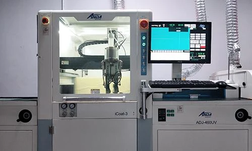
- Partnering: Working with a manufacturer like APTPCB (APTPCB PCB Factory) ensures DFM checks are tailored to harsh industrial environments.
What Clarification PCB really means (scope & boundaries)
To understand Clarification PCB design, we must first look at the systems they control. These are not standard desktop electronics. A Clarification PCB is the central nervous system for machines that separate solids from liquids or manage precise atmospheric conditions.
In industrial contexts, these boards drive the automation for sedimentation tanks, clarifiers, and filtration units. They process signals from turbidity sensors, pH probes, and flow meters, while simultaneously driving heavy loads like sludge pumps and aeration blowers.
The scope of a Clarification PCB extends beyond simple logic. It encompasses:
- Activated Sludge PCB: These are specific to biological wastewater treatment. They control the aeration cycles that keep bacteria alive to break down waste. Failure here leads to environmental non-compliance.
- Aeroponic Control PCB: Used in high-tech agriculture, these boards manage the precise misting intervals for root systems. They operate in 100% humidity environments where short circuits are a constant threat.
- Chemical Dosing Controllers: Boards that calculate and trigger the release of coagulants and flocculants to clear water.
The boundary of this technology is defined by reliability. Unlike a smartphone that can be rebooted, a Clarification PCB in a municipal water plant cannot fail without risking public health or process integrity. Therefore, the design philosophy prioritizes robustness, isolation, and longevity over miniaturization.
Clarification PCB metrics that matter (how to evaluate quality)
Building on the definition of reliability, we must quantify what makes a board "industrial grade." When specifying a Clarification PCB, generic datasheets are insufficient. You need to track specific metrics that predict failure in wet and corrosive environments.
The following table outlines the critical metrics you must control during the design and procurement phase.
| Metric | Why it matters | Typical Range / Factor | How to Measure |
|---|---|---|---|
| CTI (Comparative Tracking Index) | Measures the electrical breakdown (tracking) properties of the insulating material. High voltage + moisture = tracking. | Grade 0 (>600V) or Grade 1 (400-599V) is recommended. | IEC 60112 Standard test methods. |
| Tg (Glass Transition Temperature) | Determines when the PCB substrate turns from hard to soft. Vital for boards near hot pumps or motors. | High Tg (>170°C) is preferred for industrial clarification units. | DSC (Differential Scanning Calorimetry). |
| SIR (Surface Insulation Resistance) | Indicates cleanliness and resistance to electrochemical migration (dendrite growth). | >10^8 Ohms after humidity exposure. | IPC-TM-650 2.6.3.3 test method. |
| Copper Peel Strength | Ensures traces do not lift under thermal stress or vibration from heavy machinery. | >1.4 N/mm (standard), >1.8 N/mm (high reliability). | IPC-TM-650 2.4.8 test method. |
| Solder Mask Hardness | Protects the copper from physical abrasion and chemical attack. | >6H pencil hardness. | IPC-SM-840 qualification. |
| Ionic Contamination | Residue from manufacturing can cause corrosion in humid environments. | <1.56 µg/cm² NaCl equivalent (cleanliness standard). | ROSE testing (Resistivity of Solvent Extract). |
| Impedance Control | Critical for sensor data integrity (turbidity/flow signals) over long cable runs. | ±10% or ±5% tolerance depending on sensor interface. | TDR (Time Domain Reflectometry). |
How to choose Clarification PCB: selection guidance by scenario (trade-offs)
Once you understand the metrics, the next step is applying them to your specific use case. Not all clarification systems require the same level of protection. Over-engineering adds unnecessary cost, while under-engineering leads to field failure.
Here are six common scenarios and the recommended trade-offs for each.
1. Municipal Wastewater Treatment (Activated Sludge)
- Environment: High hydrogen sulfide (corrosive gas), outdoor temperature fluctuations, continuous operation.
- Recommendation: Use High-Tg FR4 with ENIG surface finish. A thick layer of silicone or urethane conformal coating is mandatory.
- Trade-off: Higher cost for coating and gold finish, but essential to prevent "black pad" corrosion and sulfur attack.
- Focus: Activated Sludge PCB designs must prioritize gas-tight seals on connectors.
2. Aeroponic and Hydroponic Farming
- Environment: 90-100% humidity, nutrient salts in the air, moderate temperatures.
- Recommendation: Use a rigid board with aggressive ground pours to reduce noise. Apply acrylic conformal coating (easier to rework).
- Trade-off: You can use standard Tg materials (130-140°C) since heat is rarely an issue, saving money to spend on better waterproofing.
- Focus: Aeroponic Control PCB layouts should separate high-voltage pump relays from sensitive moisture sensor inputs by at least 5mm.
3. Industrial Chemical Clarification
- Environment: Exposure to specific chemicals (acids, alkalis), controlled indoor temperature.
- Recommendation: Material selection depends on chemical compatibility. PTFE or specialized laminates may be required if the board is near fumes.
- Trade-off: Extremely high material cost. Manufacturing lead times are longer.
- Focus: Chemical resistance takes precedence over electrical speed.
4. Portable Water Quality Testing
- Environment: Handheld, battery-operated, drops/impacts, intermittent moisture.
- Recommendation: Rigid-Flex PCB to reduce connector failures. HDI (High Density Interconnect) to miniaturize.
- Trade-off: Higher manufacturing complexity and NRE (Non-Recurring Engineering) costs.
- Focus: Mechanical durability and low power consumption.
5. Desalination / Marine Clarification
- Environment: Salt spray, high UV exposure (if outdoor), vibration.
- Recommendation: Heavy copper (2oz or 3oz) for power handling. UV-stable solder mask.
- Trade-off: Fine pitch components are harder to place on heavy copper.
- Focus: Preventing salt-induced galvanic corrosion.
6. Laboratory Precision Clarification
- Environment: Controlled lab setting, low noise requirement, high precision.
- Recommendation: Standard FR4 is acceptable, but signal integrity is paramount. Use multi-layer boards with dedicated ground planes.
- Trade-off: Cost increases with layer count, but environmental protection is less critical.
- Focus: Signal-to-noise ratio (SNR) for analytical sensors.
Clarification PCB implementation checkpoints (design to manufacturing)

Selecting the right scenario is only the planning phase; execution requires a rigorous checkpoint system. When moving a Clarification PCB from CAD to the factory floor, missing a single detail can compromise the entire batch.
Use this checklist to guide your design through the manufacturing process.
1. Stack-up and Material Verification
Before routing a single trace, confirm the stack-up with your manufacturer. For high-voltage clarification systems, ensure the dielectric thickness between layers is sufficient to prevent breakdown.
- Risk: Arcing between layers.
- Action: Request a stack-up diagram from APTPCB early in the design phase.
2. Component Placement for Thermal Management
Pumps and solenoids generate heat. Place power components (MOSFETs, relays) away from sensitive analog front-ends (AFEs) used for sensor reading.
- Risk: Thermal drift affecting sensor accuracy.
- Action: Use thermal reliefs and consider heavy copper configurations for high-current paths.
3. Creepage and Clearance Rules
Standard IPC rules may not be enough for pollution degree 3 (industrial) environments. Increase spacing between high-voltage (110V/220V) and low-voltage (3.3V/5V) sections.
- Risk: Short circuits due to dust and moisture accumulation.
- Action: Apply slots (cut-outs) in the PCB between high-voltage pads to increase creepage distance.
4. Surface Finish Selection
Avoid HASL (Hot Air Solder Leveling) if fine-pitch components are used, but more importantly, avoid OSP (Organic Solderability Preservative) for harsh environments as it degrades quickly.
- Risk: Oxidation and poor solder joints over time.
- Action: Specify ENIG (Electroless Nickel Immersion Gold) or Immersion Tin for better corrosion resistance.
5. Protection of Vias
In wet environments, open vias are moisture traps.
- Risk: Water accumulation leading to barrel cracking or corrosion.
- Action: Specify "Tented Vias" or "Plugged and Capped Vias" (IPC-4761 Type VII) to seal the board surface completely.
6. Conformal Coating Strategy
Design the board with coating in mind. Leave space around connectors for masking.
- Risk: Coating wicking into connectors, rendering them useless.
- Action: clearly mark "Keep Out" zones for protective conformal coatings on the assembly drawing.
7. Test Point Accessibility
Once the board is coated, probing is difficult.
- Risk: Inability to debug or repair in the field.
- Action: Place test points on the edge or use a dedicated debug header that can be sealed later.
8. Galvanic Isolation
Ensure that the logic side (microcontroller) is galvanically isolated from the field side (sensors/actuators).
- Risk: Ground loops and voltage spikes destroying the processor.
- Action: Use optocouplers or digital isolators for all I/O lines.
9. Mechanical Mounting
Clarification tanks vibrate.
- Risk: Stress fractures in solder joints.
- Action: Add mounting holes near heavy components and use locking washers.
10. Final DFM Review
Submit your Gerber files for a Design for Manufacturing (DFM) review.
- Risk: Unmanufacturable features causing delays.
- Action: Utilize industrial control solutions expertise to catch issues before production.
Clarification PCB common mistakes (and the correct approach)
Even with a checklist, engineers often fall into specific traps when designing Clarification PCBs. These mistakes usually stem from treating industrial boards like consumer electronics.
1. Ignoring the "Micro-Climate" inside the Enclosure
- Mistake: Assuming the IP67 enclosure will keep the PCB dry forever. Seals fail, and condensation occurs internally due to temperature changes.
- Correction: Design the PCB to survive without the enclosure. Assume moisture will be present. Use heating elements (resistors) to drive out condensation if necessary.
2. Over-reliance on Autorouters
- Mistake: Letting software route sensitive analog signals next to noisy motor drivers.
- Correction: Manually route critical paths. Keep the return paths for high currents separate from sensor grounds (Star Grounding).
3. Insufficient Trace Width for Inrush Current
- Mistake: Sizing traces for steady-state current but forgetting the 3x-5x inrush current of pumps and motors.
- Correction: Use a trace width calculator with a conservative temperature rise allowance (e.g., 10°C) and add 50% safety margin.
4. Neglecting Connector Quality
- Mistake: Using cheap tin-plated headers in a sulfur-rich wastewater environment.
- Correction: Use gold-plated contacts and locking connectors (like Molex or TE industrial series) to prevent fretting corrosion.
5. Forgetting Field Maintenance
- Mistake: Soldering fuses directly to the board.
- Correction: Use fuse holders. In a clarification plant, fuses blow. If a technician needs a soldering iron to fix it, the design has failed.
6. Skipping the Burn-in Test
- Mistake: Testing the board only at room temperature.
- Correction: Perform environmental stress screening (ESS) or at least a burn-in cycle to trigger infant mortality failures before the board reaches the site.
Clarification PCB FAQ (cost, lead time, Submit your Gerber files for Design for Manufacturing (DFM) files, stackup, impedance, IPC class)
Q1: What is the best surface finish for Clarification PCBs? A: ENIG (Electroless Nickel Immersion Gold) is generally the best choice. It offers a flat surface for SMT components and excellent corrosion resistance compared to HASL or OSP.
Q2: Can I use standard FR4 for Activated Sludge PCBs? A: You can, provided the Tg (Glass Transition Temperature) is high enough for your operating environment and you apply a robust conformal coating. However, for high-reliability applications, High-Tg FR4 (Tg >170°C) is recommended to prevent delamination.
Q3: How do I protect the PCB from hydrogen sulfide gas? A: Hydrogen sulfide attacks copper and silver. You must use a conformal coating (silicone or epoxy) that is impermeable to gases. Additionally, ensure all exposed metal contacts are gold-plated.
Q4: What is the difference between an Aeroponic Control PCB and a standard timer? A: An Aeroponic Control PCB is designed to switch solenoids in millisecond bursts while resisting 100% humidity. Standard timers often lack the precision and the moisture protection required for root misting systems.
Q5: Should I use a metal core PCB (MCPCB) for clarification systems? A: Only if you are driving high-power LEDs (for UV sterilization) or very high-power motor drivers. For standard control logic, FR4 is sufficient.
Q6: How often should Clarification PCBs be replaced? A: A well-designed industrial PCB should last 10-15 years. However, electrolytic capacitors may dry out sooner. Design with high-endurance capacitors (105°C rated) to extend life.
Q7: Is potting better than conformal coating? A: Potting (encapsulating the entire board in resin) offers superior protection against vibration and moisture but makes repair impossible. Conformal coating is a balance between protection and repairability.
Q8: What data do I need to send for a quote? A: You need to provide Gerber files, the Bill of Materials (BOM), pick-and-place files, and a fabrication drawing that specifies the laminate, copper weight, color, and coating requirements.
Q9: Why is impedance control important in water treatment? A: Many modern water quality sensors use high-frequency signals or digital protocols (RS-485, Modbus). Impedance mismatches can cause signal reflection, leading to erroneous data readings.
Q10: Does APTPCB handle the assembly of these boards? A: Yes, APTPCB handles both fabrication and assembly, including the application of conformal coatings and rigorous quality standards testing required for industrial boards.
Clarification PCB glossary (key terms)
| Term | Definition |
|---|---|
| Activated Sludge | A process for treating sewage and industrial wastewaters using air and biological flocs. PCBs here control aeration. |
| Aeroponics | A method of growing plants in an air or mist environment without soil. PCBs control the misting timing. |
| BOM (Bill of Materials) | A comprehensive list of parts, items, assemblies, and other materials required to create the PCB. |
| Conformal Coating | A protective chemical coating or polymer film 25-75µm thick that 'conforms' to the circuit board topology. |
| Creepage | The shortest distance between two conductive parts along the surface of a solid insulating material. |
| DFM (Design for Manufacturing) | The practice of designing circuit boards in such a way that they are easy to manufacture. |
| Electrochemical Migration | The growth of conductive metal filaments on a PCB under the influence of a DC voltage bias and humidity. |
| ENIG | Electroless Nickel Immersion Gold. A surface finish offering good oxidation resistance and a flat surface. |
| Flocculation | A process in water clarification where solids form clusters (flocs) to be removed. |
| FR4 | A grade designation assigned to glass-reinforced epoxy laminate material. |
| Galvanic Corrosion | Damage induced when two dissimilar materials are coupled in a corrosive electrolyte (like saltwater). |
| Gerber Files | The standard file format used by the PCB industry software to describe the printed circuit board images. |
| IPC Standards | The trade association for the electronic interconnection industries that sets the standards for PCB design and assembly. |
| Tg (Glass Transition Temp) | The temperature at which the PCB base material transitions from a glassy, rigid state to a softened, deformable state. |
Conclusion (next steps)
Clarification PCB design is a discipline that sits at the intersection of electronics, chemistry, and mechanical engineering. Whether you are building a controller for an Activated Sludge plant or a precision Aeroponic Control PCB, the goal remains the same: absolute reliability in environments that are hostile to electronics.
Success lies in the details—choosing the right CTI rating, ensuring proper creepage distances, selecting the correct surface finish, and validating the design against moisture and vibration. A board that works on the test bench is not finished; it is only finished when it can survive the "micro-climate" of a clarification tank.
Ready to move to production? To ensure your Clarification PCB meets industrial standards, prepare the following for your manufacturer:
- Gerber Files (RS-274X format).
- Fabrication Drawing specifying IPC Class 2 or 3, material Tg, and coating requirements.
- Stack-up requirements (especially for impedance controlled lines).
- Test Requirements (ICT, FCT, or specific isolation tests).
At APTPCB, we specialize in high-reliability boards for industrial applications. Our engineering team reviews every design for potential failure points before production begins. Contact us today to start your DFM review and ensure your clarification system runs without interruption.