Key Takeaways
- Definition: A Clinical Information PCB is a specialized circuit board designed to capture, process, and transmit sensitive medical data with zero tolerance for error.
- Safety Standards: These boards often require adherence to IEC 60601 standards, specifically regarding isolation barriers like 2 MOOP PCB (Means of Operator Protection) requirements.
- Material Integrity: High-reliability materials are non-negotiable to prevent dielectric breakdown and ensure signal integrity during Clinical Evaluation PCB phases.
- Traceability: Every layer, component, and process step must be traceable to comply with ISO 13485 and FDA requirements.
- Testing: Automated Optical Inspection (AOI) is not enough; In-Circuit Testing (ICT) and functional validation are mandatory.
- Partnership: Working with a manufacturer like APTPCB (APTPCB PCB Factory) ensures that Design for Manufacturing (DFM) reviews catch compliance issues early.
- Lifecycle: Long-term availability of components is critical to avoid costly redesigns during the product's clinical lifespan.
What Clinical Information PCB really means (scope & boundaries)
Understanding the core definition is the first step before diving into the technical metrics of these critical components.
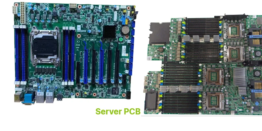
A Clinical Information PCB is not just a standard circuit board used in a hospital setting; it is the hardware foundation responsible for the acquisition and fidelity of patient data. Unlike general consumer electronics, these boards operate in environments where failure can lead to misdiagnosis or compromised patient safety. The scope of these PCBs extends from high-resolution imaging systems (MRI, CT) to wearable patient monitors and bedside infusion pumps.
The primary distinction lies in the "Information" aspect. These boards handle low-level analog signals from sensors (heart rate, blood oxygen, neural activity) and convert them into digital data for clinical decision-making. This requires exceptional signal integrity and immunity to electromagnetic interference (EMI). Furthermore, during the Clinical Evaluation PCB stage—where devices are tested on humans for regulatory approval—the hardware must perform exactly as the final production unit would. Any deviation here can invalidate clinical trial data.
APTPCB emphasizes that the boundary of these boards also includes strict isolation. If a board connects to a patient and a wall outlet, it must bridge the gap between safety extra-low voltage (SELV) and hazardous voltages, often requiring specific creepage and clearance distances.
Metrics that matter (how to evaluate quality)
Once the scope is defined, engineers must quantify quality using specific metrics that predict long-term reliability.
To ensure a Clinical Information PCB functions correctly over its intended lifespan, you must track specific physical and electrical properties. In medical electronics, "good enough" is not an acceptable standard. The following table outlines the critical metrics that drive decision-making during the engineering phase.
| Metric | Why it matters | Typical range or influencing factors | How to measure |
|---|---|---|---|
| Dielectric Constant (Dk) Stability | Ensures signal timing and integrity remain consistent, crucial for diagnostic data accuracy. | 3.0 – 4.5 (varies by frequency). Must remain stable across temp changes. | Vector Network Analyzer (VNA) or TDR. |
| Coefficient of Thermal Expansion (CTE) | Prevents barrel cracks in vias during thermal cycling (sterilization or operation). | < 50 ppm/°C (Z-axis). Lower is better for reliability. | Thermomechanical Analysis (TMA). |
| Surface Insulation Resistance (SIR) | Measures the board's resistance to electrochemical migration (dendrite growth) which causes shorts. | > 10^10 Ohms. Influenced by flux residues and cleanliness. | IPC-TM-650 2.6.3.7 test method. |
| Impedance Control Tolerance | Critical for high-speed data transfer between sensors and processors. | ±5% or ±10%. Tighter tolerance requires precise etching. | Time Domain Reflectometry (TDR). |
| Glass Transition Temp (Tg) | Determines the temperature at which the PCB material begins to soften and lose mechanical strength. | High Tg (>170°C) is preferred for clinical devices. | Differential Scanning Calorimetry (DSC). |
| Ion Chromatography (Cleanliness) | Detects ionic contamination that could cause corrosion over time in humid clinical environments. | < 1.56 µg/cm² of NaCl equivalent. | IPC-TM-650 2.3.25. |
| Peel Strength | Ensures copper traces do not lift from the substrate under thermal or mechanical stress. | > 1.05 N/mm (standard FR4). Higher for flex applications. | Tensile test equipment. |
| Leakage Current | Vital for patient safety (2 MOOP/2 MOPP) to prevent electric shock. | Microampere range (µA). Defined by IEC 60601. | Hi-Pot Tester / Dielectric Withstand test. |
Selection guidance by scenario (trade-offs)
With the metrics established, the next challenge is selecting the right board architecture for your specific clinical application.
Not all medical devices require the same PCB technology. A disposable diagnostic patch has vastly different requirements than a surgical robot. Below are common scenarios involving Clinical Information PCB designs and the necessary trade-offs engineers must navigate.
1. High-Frequency Imaging Systems (MRI/CT)
- Requirement: Extreme signal integrity and low loss.
- Trade-off: Cost vs. Performance. Standard FR4 is insufficient.
- Selection: You must use PTFE or ceramic-filled hydrocarbon materials. While expensive and harder to process, they preserve signal clarity.
- Resource: Consider Rogers PCB materials for these high-frequency applications.
2. Wearable Patient Monitors
- Requirement: Lightweight, conformable to the body, and durable against movement.
- Trade-off: Durability vs. Complexity.
- Selection: Rigid-Flex PCBs are the standard here. They eliminate heavy connectors but require careful mechanical modeling to prevent trace fracturing at the bend radius.
3. Implantable Devices (Pacemakers, Neurostimulators)
- Requirement: Miniaturization and absolute biocompatibility.
- Trade-off: Density vs. Manufacturability.
- Selection: High-Density Interconnect (HDI) with Any-Layer via structures. Materials must be biocompatible or hermetically sealed. Reliability is the only metric that matters; cost is secondary.
4. Bedside Infusion Pumps
- Requirement: Robustness and long operational life (10+ years).
- Trade-off: Technology Age vs. Availability.
- Selection: Standard multi-layer FR4 with High Tg. Avoid bleeding-edge components that might go obsolete quickly. Focus on robust power planes and thermal management.
5. Handheld Diagnostic Tools (Ultrasound, Blood Analyzers)
- Requirement: Portable power efficiency and compact size.
- Trade-off: Thermal Management vs. Size.
- Selection: PCBs with heavy copper or metal cores (IMS) may be needed to dissipate heat without bulky fans, which are undesirable in sterile environments.
6. Telemedicine & Remote Hubs
- Requirement: Connectivity (Wi-Fi, Bluetooth, 5G) and data encryption.
- Trade-off: RF Performance vs. Digital Noise.
- Selection: Mixed-signal boards where RF sections are strictly isolated from digital logic. Shielding cans and edge plating are often required to prevent EMI leakage.
From design to manufacturing (implementation checkpoints)

After selecting the right architecture, the focus shifts to the rigorous execution of the design through the manufacturing process.
Transforming a schematic into a physical Clinical Information PCB requires a disciplined approach. Missing a single checkpoint can lead to board failure during validation or, worse, in the field. Use this checklist to guide your project from design to production.
1. Schematic Validation & BOM Scrub
- Recommendation: Verify all components are active and have a long lifecycle.
- Risk: Component obsolescence forces a redesign and re-certification (very expensive).
- Acceptance: BOM health report showing 5+ years of availability.
2. Stackup Design & Material Selection
- Recommendation: Define layer stackup early with your manufacturer.
- Risk: Unbalanced copper leads to board warping during reflow.
- Acceptance: Impedance calculation report matching target Ohms.
3. Layout for Isolation (2 MOOP)
- Recommendation: Enforce strict creepage and clearance rules for 2 MOOP PCB areas (Operator Protection).
- Risk: High voltage arcing or failing safety testing (IEC 60601).
- Acceptance: DRC (Design Rule Check) report specifically for high-voltage nets.
4. DFM (Design for Manufacturing) Review
- Recommendation: Submit Gerbers to APTPCB before finalizing the design.
- Risk: Unmanufacturable features (e.g., acid traps, slivers) causing yield loss.
- Acceptance: DFM Guidelines compliance report.
5. Etching & Layer Registration
- Recommendation: Use Laser Direct Imaging (LDI) for fine lines.
- Risk: Impedance mismatch due to over/under-etching.
- Acceptance: Cross-section analysis (microsection) verifying trace width/height.
6. Plating & Surface Finish
- Recommendation: Use ENIG (Electroless Nickel Immersion Gold) for flat pads and reliability.
- Risk: Black pad syndrome or poor solderability.
- Acceptance: X-ray fluorescence (XRF) measurement of gold thickness.
7. Solder Mask & Legend
- Recommendation: Ensure mask dams are sufficient to prevent solder bridging.
- Risk: Shorts on fine-pitch components.
- Acceptance: Visual inspection and adhesion test.
8. Electrical Testing (E-Test)
- Recommendation: 100% Netlist testing (Flying Probe or Bed of Nails).
- Risk: Open circuits or shorts shipping to assembly.
- Acceptance: Certificate of Conformance (CoC) confirming 100% pass rate.
9. Cleanliness & Ionic Contamination
- Recommendation: Wash boards thoroughly to remove flux residues.
- Risk: Dendrite growth causing shorts in humid clinical settings.
- Acceptance: ROSE test or Ion Chromatography results.
10. Final Quality Audit
- Recommendation: Inspect against IPC-A-600 Class 3 standards.
- Risk: Minor defects that are acceptable in consumer goods are failures in medical.
- Acceptance: Final QC report including photos and dimensional checks.
Common mistakes (and the correct approach)
Even with a checklist, engineers often fall into specific traps when designing PCBs for clinical environments.
Avoiding these common pitfalls can save months of development time and thousands of dollars in re-spins.
Treating Medical PCBs like Consumer Electronics
- Mistake: Prioritizing cost over reliability or using IPC Class 2 standards instead of Class 3.
- Correction: Always design to IPC Class 3 (High Reliability) standards for any Clinical Information PCB. The cost of failure involves patient health, not just warranty returns.
Neglecting the "2 MOOP" Requirement
- Mistake: Failing to calculate creepage and clearance for Means of Operator Protection (MOOP) or Means of Patient Protection (MOPP).
- Correction: Use calculators based on IEC 60601-1 standards early in the layout phase. Physical slots in the PCB may be required to increase creepage distance without increasing board size.
Inadequate Thermal Management
- Mistake: Assuming standard convection cooling works inside sealed, water-resistant medical enclosures.
- Correction: Simulate thermal performance assuming zero airflow. Use heavy copper, thermal vias, and heat sinks to conduct heat to the device chassis.
Overlooking Test Points
- Mistake: Removing test points to save space, making the board impossible to validate during mass production.
- Correction: Design for Testability (DFT). If physical test points don't fit, ensure JTAG or boundary scan capabilities are accessible.
Poor Documentation for Traceability
- Mistake: Not recording batch numbers for laminate materials or solder mask.
- Correction: Maintain full traceability. If a specific batch of laminate is defective, you need to know exactly which serial numbers are affected to issue a targeted recall rather than a total recall.
Ignoring Flex Cracking
- Mistake: Placing vias or components in the bend area of a rigid-flex board.
- Correction: Keep the bend area free of plated through-holes and components. Run traces perpendicular to the bend line and use hatched copper planes to maintain flexibility.
FAQ
Having covered the technical pitfalls, here are answers to the most frequent questions regarding clinical PCB production.
Q: What is the difference between a Clinical Information PCB and a standard PCB? A: The main differences are reliability standards (IPC Class 3), stricter material requirements (cleanliness, tracking resistance), and regulatory compliance (traceability for ISO 13485).
Q: What does "2 MOOP PCB" stand for? A: It stands for "Two Means of Operator Protection." It is a safety standard defined in IEC 60601-1 that ensures the device operator is protected from electrical shock through double insulation or reinforced isolation barriers on the PCB.
Q: Why is the "Clinical Evaluation PCB" phase so critical? A: This phase involves testing the device in real-world or simulated clinical scenarios. The PCB used here must be production-quality because any changes after this phase may require re-submitting the device for regulatory approval (FDA/CE).
Q: Can I use standard FR4 for medical devices? A: Yes, for many applications like bedside monitors, high-quality FR4 is acceptable. However, for imaging (RF) or implantable devices, specialized materials are required.
Q: How do you ensure the cleanliness of medical PCBs? A: We use aggressive washing processes and measure cleanliness using Ionic Contamination testing (ROSE test) to ensure residues do not exceed strict limits.
Q: What surface finish is best for Clinical Information PCBs? A: ENIG (Electroless Nickel Immersion Gold) is the most common choice because it is lead-free, offers a flat surface for fine-pitch components, and has excellent shelf life and reliability.
Q: Does APTPCB support ISO 13485 requirements? A: Yes, we support the documentation, traceability, and quality management systems required for medical device manufacturing.
Q: How long does it take to manufacture a medical-grade PCB? A: While standard prototypes can be done in 24-48 hours, medical-grade boards often require 5-10 days due to additional testing, cross-sectioning, and quality reporting steps.
Q: What is the impact of via-in-pad technology in medical PCBs? A: Via-in-pad allows for higher component density (miniaturization), which is crucial for wearables and handhelds. It requires capping and plating over the via to ensure a flat soldering surface.
Q: How do you handle obsolescence for medical products with long lifecycles? A: We recommend a quarterly BOM health check and purchasing strategic stock of critical components or laminate materials to ensure supply continuity for 5-10 years.
Related pages & tools
- Rogers PCB Materials – Explore high-frequency materials essential for medical imaging.
- DFM Guidelines – Ensure your medical design is manufacturable before you order.
- Impedance Calculator – Verify your trace widths for accurate data transmission.
- Get a Quote – Start the review process for your clinical project.
Glossary (key terms)
To navigate the complex world of medical electronics, familiarity with these specific terms is essential.
| Term | Definition |
|---|---|
| IPC Class 3 | The highest IPC standard for PCB manufacturing, denoting "High Reliability Electronic Products" where downtime is not tolerated. |
| ISO 13485 | A quality management system standard specifically for the design and manufacture of medical devices. |
| 2 MOOP | Two Means of Operator Protection. A safety isolation requirement to protect the device user from shock. |
| 2 MOPP | Two Means of Patient Protection. Stricter than MOOP, designed to protect the patient connected to the device. |
| Clinical Evaluation | The assessment and analysis of clinical data pertaining to a medical device to verify its clinical safety and performance. |
| Creepage | The shortest distance between two conductive parts along the surface of the insulation material. |
| Clearance | The shortest distance between two conductive parts through the air. |
| HDI | High-Density Interconnect. A PCB technology using microvias and fine lines to pack more functionality into smaller spaces. |
| Bio-compatibility | The property of a material being compatible with living tissue, essential for implantable or skin-contact PCBs. |
| CTI (Comparative Tracking Index) | A measure of the electrical breakdown (tracking) properties of an insulating material. High CTI is safer. |
| UDI | Unique Device Identification. A system used to mark and identify medical devices within the healthcare supply chain. |
| CAF | Conductive Anodic Filament. A failure mode where copper filaments grow inside the PCB laminate, causing shorts. |
| Rigid-Flex | A hybrid PCB construction combining rigid and flexible substrates, common in medical wearables. |
Conclusion (next steps)
Developing a Clinical Information PCB is a balancing act between cutting-edge technology and absolute reliability. Whether you are designing for a Clinical Evaluation PCB phase or scaling up for mass production with 2 MOOP PCB safety requirements, the margin for error is non-existent.
Success relies on clear specifications, rigorous testing, and early collaboration with your manufacturing partner. When you are ready to move forward, APTPCB recommends preparing the following for a comprehensive DFM review:
- Gerber Files (RS-274X): The complete artwork for all layers.
- Fabrication Drawing: Specifying IPC Class 3, material requirements (Tg, CTI), and surface finish.
- Stackup Details: Desired layer count and impedance constraints.
- Netlist: For 100% electrical validation.
- Safety Requirements: Explicitly mark isolation areas for high-voltage protection.
By providing this data upfront, you ensure that your medical device is built on a foundation of quality, safety, and performance.