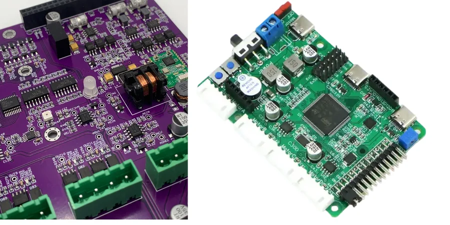
The transition to Industry 4.0 relies heavily on the hardware that powers automation, and at the center of this transformation is the Connected Factory PCB. These printed circuit boards are not merely passive carriers of electronic components; they are the active nervous system of smart manufacturing environments, facilitating real-time data exchange between machines, sensors, and cloud systems.
For engineers and procurement managers, understanding the specific requirements of a Connected Factory PCB is critical. Unlike consumer electronics, these boards must withstand harsh industrial environments while maintaining high-speed signal integrity for data transmission. APTPCB (APTPCB PCB Factory) specializes in fabricating these high-reliability boards, ensuring that the physical layer of your IoT network performs without failure.
Key Takeaways
- Definition: A Connected Factory PCB is designed specifically for Industrial IoT (IIoT), prioritizing connectivity, durability, and data integrity.
- Critical Metrics: Signal integrity (impedance control) and thermal management are the top performance indicators.
- Emerging Tech: 3D Printing PCB technology and Additive Manufacturing are increasingly used for rapid prototyping of complex sensor housings and non-planar circuits in smart factories.
- Misconception: High cost does not always equal high reliability; correct material selection matters more than raw material price.
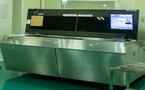
- Validation: Automated Optical Inspection (AOI) is insufficient; functional testing (FCT) is mandatory for connected devices.
- Tip: Always design the stack-up early to accommodate high-speed communication protocols like Ethernet or 5G.
What Connected Factory PCB really means (scope & boundaries)
Building on the core definition, it is essential to understand the specific scope and boundaries that separate a Connected Factory PCB from standard electronics.
A Connected Factory PCB is defined by its operating environment and its function. While a standard PCB might sit in a temperature-controlled office, a factory PCB often operates near vibrating motors, inside high-temperature ovens, or within robotic arms requiring constant flexion. The "Connected" aspect implies that the board includes RF (Radio Frequency) capabilities, Ethernet ports, or sensor arrays that feed data into a larger Manufacturing Execution System (MES).
The scope of these boards includes:
- Data Acquisition: Boards that interface with sensors (temperature, vibration, pressure).
- Communication: Boards handling Wi-Fi, Bluetooth, LoRaWAN, or 5G signals.
- Control: Boards driving actuators and motors based on received data.
Recent advancements in Additive Manufacturing have expanded this scope. Engineers can now utilize 3D Printing PCB techniques for rapid prototyping of custom sensor nodes that fit into irregular spaces within legacy machinery. This allows older factories to become "connected" without replacing heavy equipment. However, for mass production, traditional subtractive manufacturing remains the standard for reliability and conductivity.
Connected Factory PCB metrics that matter (how to evaluate quality)
Once the scope is defined, the next step is quantifying quality through specific metrics that ensure the board can handle industrial demands.
In a connected factory, a board failure leads to downtime, which is far more costly than the board itself. Therefore, metrics focus on reliability and signal preservation.
| Metric | Why it matters | Typical range or influencing factors | How to measure |
|---|---|---|---|
| Impedance Control | Ensures data signals (Ethernet/RF) do not degrade or reflect, preventing data loss. | ±5% to ±10% tolerance; dependent on trace width and dielectric height. | Time Domain Reflectometry (TDR). |
| Tg (Glass Transition Temp) | Determines the temperature at which the PCB material begins to soften and lose structural integrity. | Standard: 130°C; High-Tg: >170°C (Recommended for factories). | Differential Scanning Calorimetry (DSC). |
| CTE (Coeff. of Thermal Expansion) | Measures how much the board expands under heat. Mismatch causes solder joint cracks. | Z-axis expansion should be <3.5% (50-260°C). | Thermomechanical Analysis (TMA). |
| Dielectric Constant (Dk) | Affects signal speed and integrity, crucial for wireless communication modules. | 3.0 to 4.5 (lower is better for high-speed signals). | Resonator method or Impedance Analyzer. |
| CAF Resistance | Prevents internal short circuits caused by electrochemical migration in humid factory environments. | Material grade (e.g., CAF-resistant FR4). | High Voltage bias testing under humidity. |
How to choose Connected Factory PCB: selection guidance by scenario (trade-offs)
Understanding the metrics allows you to select the right board architecture for your specific industrial application, balancing performance against cost.
Different zones within a factory require different PCB technologies. APTPCB recommends evaluating the physical stress and data requirements of the installation site before finalizing the design.
1. Robotic Arms and Moving Machinery
- Recommendation: Rigid-Flex PCB.
- Why: These boards combine the stability of rigid boards with the flexibility of cables. They eliminate heavy connectors that can vibrate loose.
- Trade-off: Higher initial manufacturing cost vs. significantly higher reliability and reduced weight.
2. High-Temperature Processing (Ovens/Foundries)
- Recommendation: Ceramic PCB or Heavy Copper PCB.
- Why: Ceramic substrates dissipate heat efficiently, and heavy copper can carry high currents without overheating.
- Trade-off: Ceramic is brittle and expensive; Heavy Copper requires wider trace spacing.
3. Industrial Control Panels (PLCs)
- Recommendation: Industrial Control PCB (High-Tg FR4 Multilayer).
- Why: Standard multilayer boards with High-Tg materials offer the best balance of density and durability for logic processing.
- Trade-off: Standard FR4 may not handle RF signals well if the PLC includes wireless modules.
4. Remote IoT Sensors (Battery Powered)
- Recommendation: HDI (High Density Interconnect) PCB.
- Why: Miniaturization is key. HDI allows for smaller footprints, fitting into compact housings.
- Trade-off: Complex fabrication process (laser drilling) increases lead time slightly.
5. Rapid Prototyping for Custom Jigs
- Recommendation: 3D Printing PCB / Additive Manufacturing.
- Why: Allows for non-planar electronics (circuits printed directly onto curved surfaces) for immediate testing of fit and form.
- Trade-off: Lower conductivity and structural strength compared to traditional etched copper; not suitable for high-power mass production.
6. High-Speed Data Aggregation (Server/Gateway)
- Recommendation: Low-Loss Material PCB (e.g., Rogers or Megtron).
- Why: Essential for maintaining signal integrity at high frequencies (5G/Wi-Fi 6).
- Trade-off: Material cost is 3-5x higher than standard FR4.
Connected Factory PCB implementation checkpoints (design to manufacturing)
After selecting the right board type, the focus shifts to the execution phase, where rigorous checkpoints prevent costly design spins.
This phase bridges the gap between the digital design file and the physical product. Following a structured checklist ensures that the Connected Factory PCB will perform as simulated.
Checkpoint 1: Stack-up Definition
- Recommendation: Define the layer stack-up with your manufacturer before routing traces.
- Risk: Incorrect dielectric thickness will ruin impedance calculations for data lines.
- Acceptance: Manufacturer approves the stack-up diagram.
Checkpoint 2: DFM Review (Design for Manufacturing)
- Recommendation: Submit Gerbers for a DFM Guideline check early.
- Risk: Tight tolerances that work in software may fail in etching, leading to shorts.
- Acceptance: Clean DFM report with no critical violations.
Checkpoint 3: Component Sourcing for Longevity
- Recommendation: Verify the lifecycle of critical ICs. Industrial equipment lasts 10+ years; consumer chips do not.
- Risk: Component obsolescence forces a complete board redesign in 2 years.
- Acceptance: BOM (Bill of Materials) scrub confirming active status for all parts.
Checkpoint 4: Thermal Simulation
- Recommendation: Run thermal analysis to identify hot spots.
- Risk: Overheating causes delamination or sensor drift.
- Acceptance: Simulation shows junction temperatures remain below 85% of rated limits.
Checkpoint 5: Test Point Accessibility
- Recommendation: Ensure test points are accessible for ICT (In-Circuit Testing).
- Risk: Inability to debug boards on the production line.
- Acceptance: Test coverage report >90%.
Checkpoint 6: Conformal Coating Specification
- Recommendation: Specify coating type (Acrylic, Silicone, Urethane) based on chemical exposure.
- Risk: Corrosion from factory fumes or humidity destroys traces.
- Acceptance: Coating thickness and keep-out areas defined in assembly drawings.
Checkpoint 7: First Article Inspection (FAI)
- Recommendation: Produce a small pilot run before mass production.
- Risk: Systemic errors (e.g., wrong footprint rotation) affect thousands of units.
- Acceptance: FAI report signed off by engineering.
Checkpoint 8: Signal Integrity Validation
- Recommendation: Perform TDR testing on impedance-controlled lines.
- Risk: Data packet loss in the connected factory network.
- Acceptance: TDR coupons pass within tolerance.
Connected Factory PCB common mistakes (and the correct approach)
Even with strict checkpoints, specific pitfalls often trap designers working on industrial connected devices.
Moving from general implementation to specific errors helps refine the process further.
Ignoring Ground Loops:
- Mistake: Connecting analog and digital grounds improperly, causing noise in sensor data.
- Correction: Use a star ground topology or separate ground planes joined at a single point (ADC).
Over-reliance on Autorouters:
- Mistake: Letting software route critical high-speed differential pairs.
- Correction: Manually route Ethernet, USB, and RF lines to ensure length matching and impedance control.
Neglecting Mechanical Constraints:
- Mistake: Placing tall capacitors near mounting holes or connectors.
- Correction: Import the mechanical enclosure model into the ECAD tool to check for collisions (3D clearance check).
Underestimating Environmental Stress:
- Mistake: Using standard FR4 (Tg 130) in a high-vibration, high-heat environment.
- Correction: Upgrade to High-Tg PCB materials (Tg 170+) to prevent barrel cracking and pad lifting.
Forgetting the "Connected" Aspect:
- Mistake: Placing the antenna connector under a metal shield or battery.
- Correction: Maintain a strict keep-out zone around RF antennas to ensure signal range.
Skipping the Solder Paste Mask Expansion:
- Mistake: 1:1 ratio for aperture to pad, leading to solder bridging on fine-pitch components.
- Correction: Adjust stencil design for fine-pitch ICs to control solder volume.
Connected Factory PCB FAQ (cost, lead time, materials, testing, acceptance criteria)
To wrap up the technical details, here are answers to the most frequent questions regarding the procurement and validation of these boards.
Q1: How does the cost of a Connected Factory PCB compare to a standard consumer PCB? A: Connected Factory PCBs are typically 20-40% more expensive due to higher-grade materials (High-Tg), stricter impedance controls, and additional testing requirements (like CAF testing). However, the Total Cost of Ownership is lower due to reduced failure rates.
Q2: What is the typical lead time for manufacturing these boards? A: Standard lead time is 10-15 days. If specialized materials (like Rogers for RF) or complex Additive Manufacturing prototyping steps are involved, lead times may extend to 20 days. Quick-turn options are available for standard materials.
Q3: Which materials are best for Connected Factory PCBs exposed to chemicals? A: Apart from the substrate, the surface finish is critical. ENIG (Electroless Nickel Immersion Gold) is recommended over HASL because it is flat (good for fine pitch) and corrosion-resistant. Conformal coating is also mandatory for chemical resistance.
Q4: How do I define acceptance criteria for impedance control? A: You must specify the target impedance (e.g., 50Ω or 100Ω differential) and the tolerance (usually ±10%) in your fabrication notes. The manufacturer should provide a TDR report confirming these values were met on the test coupons.
Q5: Can 3D Printing PCB technology be used for the final product? A: Generally, no. 3D Printing PCB is excellent for prototyping complex shapes or embedding sensors in plastic parts, but it currently lacks the conductivity and thermal durability required for long-term industrial operation.
Q6: What testing is required for high-vibration environments? A: Beyond electrical testing, you should request or perform HALT (Highly Accelerated Life Testing) on the assembly. For the bare PCB, ensure the peel strength of the copper is verified and that via plating thickness meets IPC Class 3 standards (typically average 25µm).
Q7: Why is IPC Class 3 important for connected factories? A: IPC Class 2 is for "Dedicated Service Electronic Products" (laptops, microwaves). IPC Class 3 is for "High Reliability" products where downtime is not acceptable. Class 3 requires thicker plating in holes and stricter visual inspection criteria.
Q8: How do I handle heat dissipation in a sealed factory enclosure? A: Use Metal Core PCBs (MCPCB) or design thermal vias that transfer heat to a ground plane, which then connects to the chassis. Do not rely solely on air convection if the enclosure is sealed (IP67).
Resources for Connected Factory PCB (related pages and tools)
- Design Guidelines: DFM Guidelines
- Material Selection: High-Tg PCB Materials
- Industry Specifics: Industrial Control PCB
- Advanced Tech: Rigid-Flex PCB Capabilities
Connected Factory PCB glossary (key terms)
| Term | Definition |
|---|---|
| IIoT | Industrial Internet of Things; the network of connected devices in a factory. |
| IPC Class 3 | The highest standard for PCB reliability, used in aerospace, medical, and industrial sectors. |
| Impedance | The opposition to AC current flow; critical for maintaining signal quality in high-speed data lines. |
| Tg (Glass Transition) | The temperature where the PCB substrate changes from a rigid, glassy state to a soft, rubbery state. |
| CTE | Coefficient of Thermal Expansion; how much the material grows when heated. |
| Additive Manufacturing | Process of building objects layer by layer; used in 3D Printing PCB prototyping. |
| Gerber Files | The standard file format used to communicate PCB design data to the manufacturer. |
| BOM | Bill of Materials; the list of all components to be assembled onto the PCB. |
| FCT | Functional Circuit Testing; testing the board's actual operation rather than just electrical continuity. |
| AOI | Automated Optical Inspection; using cameras to check for assembly defects like missing parts or skew. |
| Via-in-Pad | A design technique where the via is placed directly in the component pad to save space and improve thermal management. |
| Stack-up | The arrangement of copper layers and insulating material (prepreg/core) in a multilayer PCB. |
Conclusion (next steps)
The Connected Factory PCB is the foundation of modern automation. It requires a shift in mindset from "cost-per-unit" to "reliability-per-hour." By prioritizing metrics like impedance control and thermal stability, and by selecting the right architecture—whether it's a rugged Rigid-Flex or a high-speed server board—you ensure your factory stays online.
As you move from design to production, remember that APTPCB is ready to support your transition to Industry 4.0.
To get an accurate DFM review and quote, please provide:
- Gerber Files: (RS-274X format preferred).
- Fabrication Drawing: Specifying material (Tg), surface finish, and color.
- Stack-up Requirements: Layer count and impedance constraints.
- Assembly BOM: If PCBA is required.
- Testing Requirements: Specific instructions for FCT or ICT.
Ensure your connected factory starts with a connection you can trust.