Choosing between coverlay and solder mask is the single most critical decision for the mechanical reliability and manufacturability of a flexible circuit. While solder mask offers high-density resolution for component assembly, only polyimide coverlay provides the robust dielectric strength and flexibility required for dynamic bending applications. This guide provides engineering teams and buyers with the specifications, risk assessments, and decision matrices needed to select the correct insulation method for Flex PCB designs.
Key Takeaways
- Dynamic vs. Static: Coverlay is mandatory for dynamic flexing (continuous motion); flexible solder mask is limited to static applications (bend-to-install) or rigidized areas.
- Minimum Web Width: Solder mask supports fine webs down to 0.1 mm (4 mil); standard drilled coverlay typically requires 0.6 mm to 0.8 mm webs to prevent tearing during lamination.
- Adhesive Squeeze-Out: Coverlay utilizes acrylic or epoxy adhesive which can flow 0.05 mm to 0.2 mm onto pads; designs must account for this "squeeze-out" tolerance in the annular ring.
- Dielectric Strength: Polyimide coverlay offers superior isolation (>3 kV/mil) compared to solder mask inks, making it safer for high-voltage traces.
- Cost Implications: Solder mask is generally 20–30% cheaper for high-volume production due to the photo-imageable process, whereas coverlay requires mechanical drilling, laser cutting, or die punching.
- Hybrid Approach: For complex designs, use coverlay on the flexible "tail" and solder mask on the component-dense "head" (often stiffened) to balance reliability with assembly density.
- Validation Tip: Always specify IPC-TM-650 2.4.1 (Adhesion) and IPC-TM-650 2.4.3 (Flexural Fatigue) in your acceptance criteria to verify the insulation will not crack or delaminate.
Scope, Decision Context, and Success Criteria
The choice between coverlay (a laminated layer of polyimide and adhesive) and solder mask (a printed liquid photo-imageable ink) impacts the circuit's ability to withstand mechanical stress and the manufacturer's ability to assemble components. This decision usually occurs during the stackup design phase or early DFM review.
Success Criteria:
- Flexibility Cycles: The insulation withstands the target bend cycles (e.g., >100,000 cycles for dynamic use) without cracking.
- Assembly Yield: No solder bridging on fine-pitch components (e.g., 0.5mm pitch BGAs) caused by poor insulation registration.
- Electrical Isolation: Zero dielectric breakdown between traces, verified by Hi-Pot testing.
Boundary Cases:
- Rigid-Flex Transition: In Rigid-Flex PCB designs, coverlay must extend slightly into the rigid section (typically 0.5mm–1.0mm) to protect the stress point, whereas solder mask is used on the rigid layers.
- ZIF Connectors: Zero Insertion Force (ZIF) fingers almost always require coverlay to meet the specific thickness tolerance (e.g., 0.3mm ±0.03mm) required for the connector housing.
Specifications to Define Upfront (Before You Commit)
To avoid engineering queries (EQs) and production delays, define these parameters clearly in your fabrication notes.
Technical Comparison: Coverlay vs. Flexible Solder Mask
| Feature | Polyimide Coverlay (Coverlay) | Flexible LPI Solder Mask | Best When | Trade-off |
|---|---|---|---|---|
| Flexibility | Excellent (Dynamic/Continuous) | Moderate (Static/Bend-to-install) | High-stress flexing is required. | Coverlay is more expensive and has lower resolution. |
| Min Web Width | 0.6 mm - 0.8 mm (Drilled) 0.2 mm (Laser) |
0.1 mm (4 mil) | High-density component placement (BGAs, QFNs). | Mask may crack if bent sharply (<10x radius). |
| Dielectric Strength | High (approx. 3-5 kV/mil) | Moderate (approx. 500 V/mil) | High voltage or harsh environments. | Coverlay adds thickness (25µm - 50µm). |
| Registration | ±0.2 mm (Drilled) ±0.05 mm (Laser) |
±0.05 mm (Photo-imageable) | Fine pitch SMT pads are present. | Coverlay requires larger annular rings to account for misalignment. |
| Adhesive Flow | Yes (Squeeze-out 0.05-0.2mm) | No (Liquid process) | Controlling impedance or stackup thickness is critical. | Squeeze-out can contaminate pads if not designed for. |
| Color | Amber/Yellow (Standard), Black, White | Green, Black, White, Amber, Blue | Cosmetic appearance matters. | Black coverlay is significantly more expensive than Amber. |
| Process | Lamination (Heat + Pressure) | Screen Print / Spray + UV Cure | Protecting traces in harsh chemical environments. | Lamination cycle adds thermal stress to the copper. |
| Cost | High (Tooling/Laser time) | Low (Batch process) | Budget is the primary driver for static flex. | Lower reliability in dynamic applications. |
Critical Specification Checklist
Include these 12+ points in your fabrication drawing:
- Material Type: Explicitly state "Polyimide Coverlay" or "Flexible LPI Solder Mask". Do not just say "Mask".
- Coverlay Thickness: Standard is 25µm (1 mil) PI + 25µm (1 mil) Adhesive. Thinner options (12.5µm) exist for higher flexibility.
- Adhesive Type: Specify acrylic or epoxy-based adhesive. Acrylic is standard for flex; epoxy is used for rigid-flex interfaces.
- Solder Mask Color: Green is standard; Black or White flexible masks are available but may be more brittle.
- Opening Method (Coverlay): Specify "CNC Drill", "Die Punch", or "Laser Cut". Laser is required for fine features but costs more.
- Squeeze-Out Tolerance: Define acceptable adhesive squeeze-out (e.g., "Max 0.2mm onto pad, 0% on contact area").
- Minimum Web: Ensure design meets the minimum web for the chosen material (e.g., 0.1mm for mask, 0.6mm for drilled coverlay).
- Annular Ring: For coverlay, increase pad size by 0.25mm (10 mil) over the drill diameter to account for registration and squeeze-out.
- Dam/Bridge Requirements: If individual solder dams are needed between pads, use solder mask or laser-cut coverlay.
- Cure Requirements: For solder mask, specify "Flexible formulation" to ensure the ink isn't standard rigid FR4 ink.
- Surface Finish Compatibility: Ensure the mask/coverlay is compatible with ENIG, ENEPIG, or Immersion Silver.
- Stiffener Integration: Define if coverlay goes under or over the stiffener. (Usually under). See how to design stiffener for flex pcb for details.
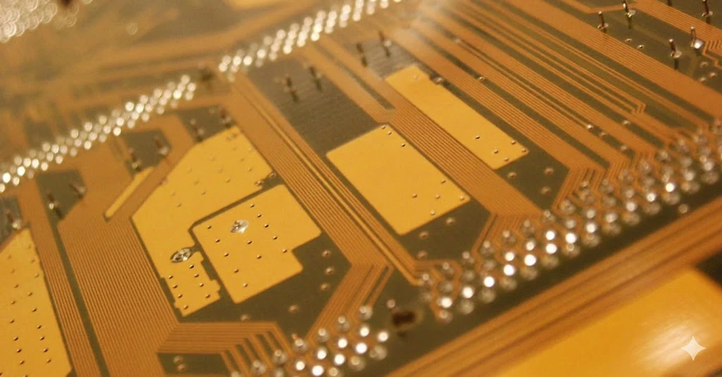
Figure 1: Complex multi-layer flex stackup. Note the use of coverlay on inner flex layers for dielectric separation.
Related resources
Key Risks (Root Causes, Early Detection, Prevention)
Failure to select the right insulation leads to field failures. Here are the top risks managed by a competent flex PCB manufacturer.
Pad Contamination (Squeeze-Out)
- Root Cause: During lamination, coverlay adhesive flows onto the SMT pad.
- Detection: Visual inspection (microscope) or poor solder wetting during assembly.
- Prevention: Design coverlay openings 0.2mm larger than the pad; use "low-flow" adhesive pre-pregs; use laser cutting for tighter tolerance.
Solder Mask Cracking
- Root Cause: Using standard rigid LPI ink on a flex board, or bending a flexible LPI beyond its elongation limit.
- Detection: Mandrel bend test (IPC-TM-650 2.4.3); visual cracks after reflow.
- Prevention: Specify "Flexible LPI" (e.g., Taiyo PSR-9000 series); restrict mask to static areas; use coverlay for dynamic zones.
Air Entrapment (Bubbles/Voiding)
- Root Cause: Uneven copper topography (e.g., 2oz copper) preventing coverlay adhesive from filling gaps.
- Detection: Visual inspection (white spots between traces); cross-section analysis.
- Prevention: Use adequate adhesive thickness (e.g., 50µm adhesive for 35µm copper); use vacuum lamination.
Registration Failure (Drill vs. Pad)
- Root Cause: Material shrinkage/expansion of Polyimide during processing (can be 0.1% - 0.3%).
- Detection: Breakout of the opening; exposed dielectric on the pad.
- Prevention: Use laser direct imaging (LDI) for mask; use laser cutting for coverlay; apply scaling factors to artwork based on material stability.
Trace Fracture at Coverlay Edge
- Root Cause: Stress concentration where the coverlay ends and the exposed pad begins.
- Detection: Open circuit after vibration testing.
- Prevention: Use "teardrop" pad shapes; anchor pads with coverlay overlap; avoid stopping coverlay exactly at a stress point.
Incomplete Development (Solder Mask)
- Root Cause: Old ink or improper UV exposure energy.
- Detection: Mask residue on pads (Scumming); poor solderability.
- Prevention: Supplier process control (Stouffer step wedge test); fresh ink usage.
ZIF Connector Thickness Mismatch
- Root Cause: Incorrect coverlay thickness calculation (ignoring adhesive flow or copper thickness).
- Detection: Connector is too loose or too tight; contact failure.
- Prevention: Perform a stackup calculation including pressed thickness; specify tolerance ±0.03mm or ±0.05mm for the contact area.
Gold Embrittlement (ENIG)
- Root Cause: Solder mask residue preventing proper Nickel/Gold plating, or "Black Pad".
- Detection: Brittle solder joints; shear test failure.
- Prevention: Ensure clean development of mask/coverlay before plating; use aggressive desmear/plasma cleaning.
Validation & Acceptance (Tests and Pass Criteria)
Do not rely on "standard inspection." Define these specific tests for your flex PCB material selection.
Acceptance Criteria Table
| Test Item | Method | Pass Criteria | Sampling |
|---|---|---|---|
| Visual Inspection | IPC-6013 Class 2/3 | No bubbles, wrinkles, or cracks. Squeeze-out < 0.2mm (or per drawing). | 100% |
| Tape Test (Adhesion) | IPC-TM-650 2.4.1 | Rating 5B (0% removal of mask/coverlay). | 2 panels / lot |
| Solder Float | IPC-TM-650 2.4.13 | 10 sec @ 260°C or 288°C. No blistering/delamination. | 1 coupon / lot |
| Dielectric Withstand | IPC-TM-650 2.5.7 | No breakdown at specified voltage (e.g., 500V DC). | 100% (Net list) |
| Flexural Fatigue | IPC-TM-650 2.4.3 | No cracks in copper or insulation after X cycles (e.g., 10k). | First Article (FAI) |
| Dimensional Check | Caliper / OGP | Coverlay openings within ±0.1mm (or ±0.05mm laser). | AQL 1.0 |
Validation Tip: For dynamic applications, request a "Flex Endurance Test" report from the manufacturer using your specific stackup (copper type + coverlay thickness). Rolled annealed vs electro-deposited copper behavior changes significantly under coverlay compression.
Supplier Qualification Checklist (RFQ, Audit, Traceability)
When vetting a manufacturer for coverlay/mask capabilities, ask:
- Cutting Capability: Do they have in-house UV or CO2 lasers for coverlay cutting? (Essential for fine pitch).
- Lamination Press: Do they use vacuum hydraulic presses or autoclaves? (Vacuum is required to remove air bubbles in coverlay).
- Material Stock: Do they stock major brands (Dupont Pyralux, Panasonic Felios) or generic equivalents?
- Registration Accuracy: Can they demonstrate ±0.05mm registration for laser-cut coverlay?
- Solder Mask Ink: Which specific "Flexible LPI" ink series do they use? (Verify datasheet for bend radius).
- Plasma Cleaning: Do they perform plasma treatment before coverlay lamination to ensure adhesion?
- DFM Support: Will they provide a "squeeze-out" analysis on the Gerber files?
- Traceability: Can they trace the specific batch of adhesive/PI used to the finished PCB lot?
- Impedance Control: Do they account for the dielectric constant difference between Coverlay (Dk ~3.4) and Solder Mask (Dk ~3.5-4.0)?
- Stiffener Alignment: Do they have automated optical alignment for attaching stiffeners over the coverlay?
- Change Control: Will they notify you before changing the adhesive brand or thickness?
- Certifications: ISO 9001 is minimum; AS9100 or ISO 13485 for aerospace/medical.
How to Choose (Trade-Offs and Decision Rules)
Use this logic to finalize your decision between coverlay and solder mask.
Decision Matrix
| Priority | Best Choice | Why |
|---|---|---|
| Dynamic Flexibility | Coverlay | Polyimide withstands millions of flex cycles; mask cracks quickly. |
| High Density (Fine Pitch) | Solder Mask (or Laser Coverlay) | Mask allows 0.1mm webs; standard coverlay requires 0.6mm+ webs. |
| Cost | Solder Mask | Photo-process is faster and cheaper than drilling/laminating coverlay. |
| High Voltage | Coverlay | Superior dielectric strength and isolation properties. |
| Harsh Environment | Coverlay | Laminated PI is more chemically resistant than printed ink. |
10 Rules for Selection
- If the flex circuit will bend continuously (dynamic), choose Polyimide Coverlay.
- If the flex circuit is "bend-to-install" (static) and cost is critical, choose Flexible LPI Solder Mask.
- If you have fine-pitch components (e.g., 0.5mm BGA) on the flex, choose Solder Mask (or Laser-Cut Coverlay if budget permits).
- If you need defined solder dams between closely spaced pads, choose Solder Mask.
- If the application involves high voltage (>500V), choose Coverlay for better insulation.
- If the copper thickness is heavy (>2 oz), choose Coverlay with thick adhesive (2-3 mil) to encapsulate traces without voids.
- If you are designing a ZIF connector interface, choose Coverlay to maintain precise thickness and friction properties.
- If you need a black matte finish for optical reasons, choose Black Coverlay (but verify cost premium).
- If the design is a Rigid-Flex, choose Coverlay for the flex section and Solder Mask for the rigid section.
- If you need the absolute smallest form factor, choose Laser-Cut Coverlay to minimize annular rings and webs.
Boundary Exceptions:
- Exception 1: Even in dynamic applications, you can use solder mask if the masked area is fully stiffened and never bends.
- Exception 2: You can combine both. Use "Selective Coverlay" for the main flex body and add "Selective Solder Mask" only around the fine-pitch component footprint (often called "Bikini Coverlay").
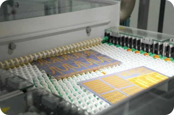
Figure 2: Adhesiveless copper clad laminate. When using coverlay with this material, the adhesive comes solely from the coverlay layer.
FAQ (Cost, Lead Time, DFM Files, Materials, Testing)
1. Can I use standard rigid solder mask on a flex PCB to save money? No. Standard rigid mask is brittle and will crack upon the first bend, potentially severing the underlying copper traces. Always specify "Flexible LPI" or coverlay.
2. How much more expensive is laser-cut coverlay compared to drilled coverlay? Laser cutting is typically 30–50% more expensive than CNC drilling/punching due to slower machine time.
Glossary (Key Terms)
| Term | Meaning | Why it matters in practice |
|---|---|---|
| DFM | Design for Manufacturability: layout rules that reduce defects. | Prevents rework, delays, and hidden cost. |
| AOI | Automated Optical Inspection used to find solder/assembly defects. | Improves coverage and catches early escapes. |
| ICT | In-Circuit Test that probes nets to verify opens/shorts/values. | Fast structural test for volume builds. |
| FCT | Functional Circuit Test that powers the board and checks behavior. | Validates real function under load. |
| Flying Probe | Fixtureless electrical test using moving probes on pads. | Good for prototypes and low/medium volume. |
| Netlist | Connectivity definition used to compare design vs manufactured PCB. | Catches opens/shorts before assembly. |
| Stackup | Layer build with cores/prepreg, copper weights, and thickness. | Drives impedance, warpage, and reliability. |
| Impedance | Controlled trace behavior for high-speed/RF signals (e.g., 50Ω). | Avoids reflections and signal integrity failures. |
| ENIG | Electroless Nickel Immersion Gold surface finish. | Balances solderability and flatness; watch nickel thickness. |
| OSP | Organic Solderability Preservative surface finish. | Low cost; sensitive to handling and multiple reflows. |
Related resources
Conclusion
coverlay vs solder mask on flex pcb Is Easiest to Get Right When You Define the Specifications and Verification Plan Early, Then Confirm Them Through DFM and Test Coverage.
Use the rules, checkpoints, and troubleshooting patterns above to reduce iteration loops and protect yield as volumes increase.
If you’re unsure about a constraint, validate it with a small pilot build before locking the production release.