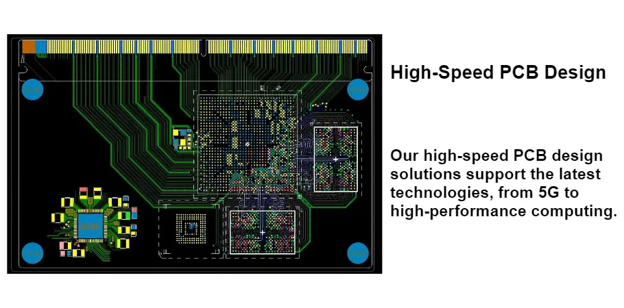
Scaling CXL 3.0 interface PCB mass production requires a rigorous shift from standard fabrication methods to ultra-precision manufacturing. With data rates hitting 64 GT/s using PAM4 signaling, the margin for error in impedance control, material selection, and drilling tolerances is virtually zero. This guide provides the specific numeric limits, process controls, and verification steps necessary to achieve high yield and signal integrity in volume production.
Quick Answer (30 Seconds)
- Critical Rule: Maintain differential impedance at 85Ω ±5%; standard ±10% tolerance is insufficient for CXL 3.0 PAM4 signaling.
- Material Requirement: Use Ultra-Low Loss materials (e.g., Megtron 7/8, Tachyon 100G) with Df < 0.002 at 10 GHz.
- Key Pitfall: Via stubs longer than 6 mil (0.15 mm) create fatal resonances; backdrilling is mandatory for thick backplanes.
- Verification: Implement 100% TDR testing on coupons and random sampling on actual boards for insertion loss verification.
- Boundary Case: If trace length exceeds 10 inches, consider low-roughness copper (HVLP/VLP, Rz < 2 µm) to minimize skin effect losses.
- DFM Item: Specify backdrill depth tolerance of ±2 mil to ensure stubs are removed without damaging internal signal layers.
Highlights
- PAM4 Sensitivity: CXL 3.0 uses Pulse Amplitude Modulation (4-level), reducing the signal-to-noise ratio (SNR) compared to NRZ.
- Stackup Precision: Layer-to-layer registration must be within 3 mil to prevent impedance discontinuities.
- Drilling Tech: High aspect ratio vias (up to 20:1) require advanced mechanical drilling or laser drilling techniques.
- Surface Finish: ENIG or ENEPIG is preferred for flatness; HASL is prohibited due to uneven surfaces affecting high-frequency signals.
- Cleanliness: Ionic contamination must be strictly controlled to prevent electrochemical migration (ECM) in high-density designs.
- Testing: VNA (Vector Network Analyzer) testing up to 32 GHz is often required for channel characterization.
Contents
- Definition and Scope (What It Is, What It Isn’t)
- Rules and Specifications (Key Parameters and Limits)
- Implementation Steps (Process Checkpoints)
- Troubleshooting (Failure Modes and Fixes)
- How to Choose (Design Decisions and Trade-Offs)
- FAQ (Cost, Lead Time, Materials, Testing, Acceptance Criteria)
- Glossary (Key Terms)
- Request a Quote (DFM Review + Pricing)
- Conclusion (next steps)
Definition and Scope (What It Is, What It Isn’t)
Applies when:
- Manufacturing server motherboards, accelerator cards, or memory expansion modules supporting the Compute Express Link (CXL) 3.0 standard.
- Designs utilize PCIe 6.0 physical layer technology running at 64 GT/s.
- The PCB stackup involves 12 to 32+ layers, often requiring high-density interconnect (HDI) or thick backplane structures.
- Signal integrity requirements demand Ultra-Low Loss (ULL) laminates and tight impedance control.
- Production volumes range from small pilot runs (NPI) to full mass production PCB manufacturing.
Doesn’t apply when:
- Designing for CXL 1.0/1.1 or PCIe 4.0/5.0 (32 GT/s NRZ), where standard Low Loss materials might suffice.
- The interface speed is below 16 GT/s, allowing for wider tolerances (±10% impedance).
- Using standard FR-4 materials (Tg 130-150°C) which have too high a Dissipation Factor (Df > 0.015) for these frequencies.
- The board is a simple 2-6 layer consumer electronics PCB without controlled impedance requirements.
Rules and Specifications (Key Parameters and Limits)
Achieving CXL 3.0 compliance in mass production requires strict adherence to physical and electrical parameters. The following table outlines the non-negotiable rules for fabrication.
| Rule | Recommended Value/Range | Why it matters | How to verify | If ignored |
|---|---|---|---|---|
| Differential Impedance | 85Ω ± 5% | CXL 3.0/PCIe 6.0 spec requires 85Ω to minimize return loss. | TDR (Time Domain Reflectometry) on test coupons. | Signal reflections cause high Bit Error Rate (BER) and link training failures. |
| Material Loss (Df) | < 0.002 @ 10 GHz | High-frequency signal attenuation must be minimized for 64 GT/s. | IPC-TM-650 2.5.5.5 test method or material datasheet cert. | Excessive insertion loss closes the signal eye diagram; link fails to negotiate speed. |
| Copper Roughness | Rz < 2.0 µm (HVLP/VLP) | Skin effect at 16-32 GHz pushes current to the surface; rough copper increases loss. | SEM (Scanning Electron Microscope) analysis of foil. | Increased insertion loss and phase distortion. |
| Via Stub Length | < 6 mil (0.15 mm) | Stubs act as antennas/filters, causing resonance dips in the frequency response. | Cross-section analysis or X-Ray inspection. | Resonances at Nyquist frequency destroy signal integrity. |
| Intra-Pair Skew | < 5 ps | Differential signals must arrive simultaneously to maintain common-mode rejection. | VNA measurement or flight time simulation. | Mode conversion (Diff to Common) and closed eye width. |
| Backdrill Depth Tolerance | ± 2 mil (0.05 mm) | Ensures the stub is removed without cutting into the active internal layer. | X-Ray inspection of backdrilled holes. | Either remaining stub is too long (fail) or active trace is severed (open circuit). |
| Layer Registration | ± 3 mil | Misalignment affects impedance and can cause shorts in high-density BGA fields. | X-Ray drill verification and microsectioning. | Impedance discontinuities and potential electrical shorts. |
| Solder Mask Web | Min 3 mil (0.075 mm) | Prevents solder bridging on fine-pitch CXL connector footprints. | AOI (Automated Optical Inspection). | Solder bridges during assembly; short circuits. |
| Plating Aspect Ratio | Max 20:1 | Ensures sufficient copper thickness in the barrel of deep vias. | Cross-section (microsection) analysis. | Barrel cracks during reflow; intermittent open circuits. |
Implementation Steps (Process Checkpoints)
Transitioning a CXL 3.0 design into mass production involves specific process controls.
1. Material Selection and Verification
- Action: Select materials like Panasonic Megtron 7/8, Isola Tachyon 100G, or equivalent.
- Check: Verify the specific prepreg glass style (e.g., 1035, 1067) to ensure resin content prevents "fiber weave effect" skew.
- Acceptance: Dk tolerance ±0.05; Df < 0.002.
2. Stackup and Impedance Modeling
- Action: Use a 2D/3D field solver (e.g., Polar SI9000) to calculate trace widths.
- Check: Account for resin flow and copper pressing thickness. For CXL 3.0, 85Ω traces are often slightly wider than standard 100Ω traces.
- Acceptance: Simulation results must match the 85Ω target within ±1Ω before fabrication begins. See our PCB stackup guide.
3. Inner Layer Imaging and Etching
- Action: Use Laser Direct Imaging (LDI) for high precision.
- Check: Etch compensation factors must be precise. Trace width tolerance should be controlled to ±0.5 mil or better.
- Acceptance: AOI inspection must show no "neck-downs" or protrusions on high-speed lines.
4. Lamination and Registration
- Action: Use Pin-lam or optical alignment systems for high layer counts (20+ layers).
- Check: X-ray verify layer alignment post-lamination.
- Acceptance: Layer-to-layer registration within 3 mil to ensure via pads hit target layers centrally.
5. Drilling and Backdrilling
- Action: Drill through-holes followed by controlled-depth backdrilling to remove stubs.
- Check: Verify drill bit life management to prevent hole wall roughness.
- Acceptance: Backdrill depth must be within ±2 mil of the target layer.
6. Plating and Surface Finish
- Action: Apply high-throw power copper plating to ensure barrel integrity in high aspect ratio vias.
- Check: Measure copper thickness in the center of the via barrel (min 0.8 mil / 20 µm).
- Acceptance: Surface finish (ENIG/ENEPIG) must be flat for high-density connector assembly.
7. Electrical Testing (TDR & VNA)
- Action: Perform 100% net list testing and TDR impedance testing on coupons.
- Check: For CXL 3.0, VNA testing on a sample basis (e.g., SET2DIL) measures insertion loss per inch.
- Acceptance: Impedance 85Ω ±5%; Loss < budget (e.g., -0.9 dB/inch @ 16 GHz).
Troubleshooting (Failure Modes and Fixes)
In CXL 3.0 interface PCB assembly, failures often manifest as signal integrity issues rather than simple opens/shorts.
Symptom 1: High Bit Error Rate (BER) or Link Flapping
- Likely Cause: Excessive via stub length causing resonance.
- Check: X-ray the backdrilled vias. Is the remaining stub > 6 mil?
- Fix: Adjust backdrill depth settings.
- Prevention: Specify "Must Not Cut" layers clearly in ODB++ data and increase backdrill clearance.
Symptom 2: Impedance consistently low (e.g., 78Ω instead of 85Ω)
- Likely Cause: Trace width is too wide or dielectric is thinner than calculated.
- Check: Cross-section the board. Measure actual trace width (top and bottom) and dielectric height.
- Fix: Adjust etch compensation factors for the next batch.
- Prevention: Perform a "first article" microsection before running the full mass production lot.
Symptom 3: Eye Diagram Closure (Vertical)
- Likely Cause: High insertion loss due to material or copper roughness.
- Check: Verify the material batch (is it actually Megtron 7?). Check copper foil roughness (is it HVLP?).
- Fix: Switch to smoother copper foil or lower loss material.
- Prevention: Mandate material certificates (CoC) with every shipment.
Symptom 4: Skew-induced Jitter
- Likely Cause: Fiber weave effect (glass bundles aligning with traces).
- Check: Inspect the glass style used (106 vs 1080 vs 1035).
- Fix: Rotate the design 10 degrees (Zig-zag routing) or use "spread glass" styles.
- Prevention: Specify spread glass FR4 or equivalent high-end glass styles in the fab notes.
Symptom 5: BGA Pad Cratering or Lifted Pads
- Likely Cause: Brittle laminate material combined with mechanical stress.
- Check: Review the Tg and CTE (Coefficient of Thermal Expansion) of the material.
- Fix: Use materials with lower Z-axis CTE or improve resin toughness.
- Prevention: Optimize the BGA/QFN fine pitch reflow profile to reduce thermal shock.
How to Choose (Design Decisions and Trade-Offs)
Making the right choices early in the design phase saves cost and improves yield in mass production PCB manufacturing.
If trace length is < 5 inches:
- Choose: Mid-loss materials (e.g., Megtron 6 or IT-968) might suffice if the loss budget permits.
- Trade-off: Saves material cost but reduces margin.
If trace length is > 10 inches:
- Choose: Ultra-Low Loss materials (Megtron 7/8, Tachyon 100G) and HVLP copper.
- Trade-off: Higher material cost, but necessary for CXL 3.0 compliance.
If layer count is > 20 layers:
- Choose: High-Tg (> 180°C) and Low-CTE materials.
- Trade-off: Prevents barrel cracks and pad cratering during multiple reflow cycles.
If routing density is extreme (0.4mm pitch BGA):
- Choose: HDI PCB technology with stacked microvias.
- Trade-off: Higher cost than through-hole, but improves signal integrity by reducing stubs naturally.
If using press-fit connectors:
- Choose: Tighter hole tolerance (+0.05/-0.05 mm) and hard gold or immersion tin finish if specified.
- Trade-off: Requires precise drill bit management.
If budget is tight but performance is critical:
- Choose: Hybrid stackup (ULL material for high-speed layers, standard FR4 for power/ground/low-speed).
- Trade-off: Complex lamination cycle; risk of warpage due to CTE mismatch.
FAQ (Cost, Lead Time, Materials, Testing, Acceptance Criteria)
Q: How much does backdrilling add to the cost of CXL 3.0 PCBs? A: Backdrilling typically adds 10-20% to the bare board cost. It requires a separate NC drill program, specialized depth-control machines, and additional inspection steps (X-ray).
Q: What is the typical lead time for Ultra-Low Loss materials? A: Materials like Megtron 7 or Tachyon often have lead times of 2-4 weeks if not in stock. For quick turn PCB needs, check stock availability immediately.
Q: Is 100% VNA testing required for mass production? A: No, 100% VNA testing is too slow and costly. Typically, we perform 100% TDR (Impedance) and use statistical sampling (e.g., 1 panel per lot) for VNA insertion loss verification.
Q: Can we use standard FR4 for CXL 3.0 designs? A: No. Standard FR4 has a Df of ~0.020, which causes massive signal loss at 16 GHz (Nyquist for 32 GT/s) and 32 GHz (Nyquist for 64 GT/s). You must use materials with Df < 0.005.
Q: What is the minimum trace width for 85Ω impedance? A: It depends on the stackup, but typically 4-5 mil (0.10-0.127 mm) for striplines. Narrower traces increase skin effect loss; wider traces require thicker dielectrics.
Q: How do you handle fiber weave effect in production? A: We use "spread glass" (mechanically spread fibers) or route traces at a slight angle (e.g., 10°) relative to the weave. This averages out the Dk variations.
Q: What surface finish is best for CXL 3.0? A: ENIG (Electroless Nickel Immersion Gold) or ENEPIG. They provide a flat surface for fine-pitch components and do not add significant loss like HASL.
Q: What is the acceptance criteria for impedance in mass production? A: IPC Class 2 or 3 usually defaults to ±10%, but for CXL 3.0, you must specify ±5% in your fabrication notes and master drawing.
Glossary (Key Terms)
| Term | Meaning | Why it matters in practice |
|---|---|---|
| PAM4 | Pulse Amplitude Modulation (4-level). | Encodes 2 bits per UI. Requires higher SNR and linearity than NRZ. |
| UI (Unit Interval) | The time duration of one bit (or symbol). | At 64 GT/s, the UI is extremely short (~15.6 ps), leaving little margin for jitter. |
| Insertion Loss (IL) | Signal power loss as it travels down the trace. | The primary limiter of trace length. Must be carefully budgeted (e.g., -30 dB total channel). |
| Return Loss (RL) | Signal power reflected back to the source. | Caused by impedance mismatches. High RL degrades the signal eye. |
| Backdrilling | Removing the unused portion of a plated through-hole (stub). | Essential |
Conclusion
CXL 3.0 interface PCB mass production is easiest to get right when you define the specifications and verification plan early, then confirm them through DFM and test coverage.
Use the rules, checkpoints, and troubleshooting patterns above to reduce iteration loops and protect yield as volumes increase.
If you’re unsure about a constraint, validate it with a small pilot build before locking the production release.