Definition, scope, and who this guide is for
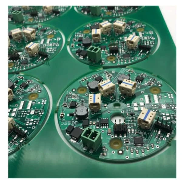
A data-center Ultrasound probe interface PCB is a specialized interconnect board designed to bridge high-channel-count ultrasound transducers with high-performance computing (HPC) backends located in server environments. Unlike standard portable ultrasound electronics, these boards are engineered for massive data throughput, continuous 24/7 operation, and integration into rack-mounted diagnostic systems or remote imaging gateways. They must handle sensitive analog signals from the probe while simultaneously managing high-speed digital serialization (often PCIe or optical) for data center processing.
This guide is written for Hardware Engineers, NPI Managers, and Procurement Leads who are tasked with sourcing these complex hybrid boards. You are likely dealing with a convergence of medical-grade precision (ISO 13485 requirements) and server-grade reliability (IPC Class 3 for high-reliability infrastructure). The decision context here involves balancing signal integrity for hundreds of piezoelectric channels against the thermal and mechanical constraints of a data center rack environment.
By following this playbook, you will move from a conceptual design to a validated manufacturing process. We cover the specific material requirements to prevent signal loss, the manufacturing risks unique to high-voltage pulser circuits, and the exact questions you need to ask a manufacturer like APTPCB (APTPCB PCB Factory) to ensure your boards pass validation on the first run.
When to use this approach (and when not to)
Determining whether you need a specialized data-center grade interface versus a standard medical PCB depends heavily on the data volume and processing location.
Use a data-center Ultrasound probe interface PCB when:
- Remote Processing: The raw RF data from the transducer is being sent to a centralized server or cloud edge for AI-driven image reconstruction, requiring massive bandwidth.
- High Channel Count: You are utilizing matrix arrays (1000+ elements) that require high-density interconnects (HDI) and high-speed serialization that standard cart-based PCBs cannot support thermally.
- Continuous Operation: The equipment is part of an automated scanning facility or research cluster running 24/7, demanding server-grade materials (High Tg) to prevent thermal degradation.
- Mixed Signal Complexity: The board must isolate high-voltage transmit pulses (up to 100V) from extremely sensitive microvolt-level receive echoes within a compact server blade form factor.
Stick to a standard medical PCB approach when:
- Portable/Point-of-Care: The device is battery-powered and handheld; power consumption is a higher priority than raw data throughput.
- On-Device Processing: Image reconstruction happens locally on an FPGA within the cart, eliminating the need for high-speed data center interconnect protocols.
- Standard Arrays: You are using standard 128-element linear probes where conventional FR4 materials suffice for signal integrity.
Specs to define (materials, stackup, tolerances)
Defining the correct specifications upfront is the only way to avoid costly re-spins. A data-center Ultrasound probe interface PCB requires a hybrid build that supports both analog fidelity and digital speed.
- Base Material (Hybrid Stackup): Use a combination of high-frequency laminates (e.g., Rogers 4350B or Panasonic Megtron 6) for signal layers and high-Tg FR4 (Tg > 170°C) for power/ground layers to balance cost and performance.
- Dielectric Constant (Dk): Target a low and stable Dk (3.4–3.6) for high-speed digital lines to minimize propagation delay and signal skew.
- Dissipation Factor (Df): Ultra-low loss (Df < 0.005 @ 10GHz) is mandatory to preserve the integrity of raw ultrasound data streams over long traces.
- Layer Count & HDI: Typically 12–24 layers. Expect 2+N+2 or 3+N+3 HDI structures with blind and buried vias to fan out high-density connector pins (0.4mm or 0.5mm pitch).
- Copper Weight: Mixed copper weights are common; 0.5oz for fine-line signal layers (impedance control) and 2oz for power planes handling the current surges of the transmit pulsers.
- Impedance Control: Strict ±5% tolerance on single-ended (50Ω) and differential pairs (85Ω or 100Ω) is required for PCIe or optical transceiver interfaces.
- Surface Finish: ENEPIG (Electroless Nickel Electroless Palladium Immersion Gold) is preferred for wire bonding reliability and excellent solderability of BGA components.
- Thermal Reliability: Material must withstand 5+ lamination cycles and lead-free reflow temperatures (260°C) without delamination (T260 > 60 min).
- CAF Resistance: Materials must be certified CAF-resistant (Conductive Anodic Filament) due to the high-voltage bias present in ultrasound pulser circuits.
- Via Aspect Ratio: For thick backplanes (up to 3.0mm), ensure the manufacturer can plate high aspect ratio vias (10:1 or 12:1) reliably.
- Cleanliness: Ionic contamination must be strictly controlled (< 1.56 µg/cm² NaCl equivalent) to prevent electrochemical migration under high voltage.
- Marking: High-contrast, permanent laser marking for traceability, including QR codes linking to manufacturing test data.
Manufacturing risks (root causes & prevention)
The convergence of high voltage and high speed creates unique failure modes. Understanding these risks allows you to preempt them during the DFM phase.
Crosstalk (Analog-Digital Interference):
- Root Cause: Placing sensitive analog receive lines too close to high-speed digital data lanes or switching power supplies.
- Detection: Signal-to-Noise Ratio (SNR) degradation in image quality.
- Prevention: Enforce strict guard traces and ground stitching vias; use separate ground planes for analog and digital sections.
Impedance Discontinuity at Vias:
- Root Cause: Improper via stub lengths or lack of back-drilling on thick server-grade boards.
- Detection: Signal reflection seen on TDR (Time Domain Reflectometry).
- Prevention: Specify back-drilling for all high-speed vias exceeding a certain stub length (e.g., >10 mils).
CAF Growth (Short Circuits):
- Root Cause: High voltage bias (transmit pulses) combined with moisture absorption in the laminate glass weave.
- Detection: Intermittent shorts or leakage current over time.
- Prevention: Use "spread glass" or flat glass weaves and CAF-resistant resin systems; increase clearance between high-voltage nets.
BGA Warpage and Open Joints:
- Root Cause: CTE mismatch between the large PCB and large FPGA/ASIC packages during reflow.
- Detection: Head-in-pillow defects or open circuits on X-ray inspection.
- Prevention: Balance copper distribution on all layers; use low-CTE laminate materials.
Plated Through Hole (PTH) Fatigue:
- Root Cause: Thermal cycling in a data center environment causes barrel cracks in high-aspect-ratio vias.
- Detection: Resistance changes during thermal shock testing.
- Prevention: Ensure minimum copper plating thickness in hole walls is >25µm (Class 3 requirement).
Surface Finish Oxidation:
- Root Cause: Poor storage or handling of ENIG/ENEPIG pads before assembly.
- Detection: Poor wetting or "black pad" syndrome.
- Prevention: Vacuum packaging with desiccant and humidity indicator cards; strict shelf-life monitoring.
Layer Misregistration:
- Root Cause: Material movement during lamination of complex hybrid stackups.
- Detection: Breakout of drill holes on internal pads (X-ray or cross-section).
- Prevention: Use pin-lamination techniques and X-ray optimization for drilling alignment.
Residue under Low-Standoff Components:
- Root Cause: Flux residue trapped under fine-pitch BGAs or connectors.
- Detection: Leakage current or corrosion over time.
- Prevention: Implement rigorous wash processes with saponifiers and cleanliness testing (Rose test).
Validation & acceptance (tests and pass criteria)

Validation must go beyond standard electrical testing. You need a test plan that simulates the stress of both the medical application and the data center environment.
- Impedance Verification (TDR):
- Objective: Confirm signal integrity for high-speed lines.
- Method: Test coupons and in-circuit traces using TDR.
- Criteria: All controlled impedance lines must be within ±5% (or ±10% if specified) of target.
- High-Potential (Hi-Pot) Testing:
- Objective: Verify isolation between high-voltage transmit nets and low-voltage logic/user-accessible parts.
- Method: Apply 2x max operating voltage + 1000V (or per standard) for 60 seconds.
- Criteria: Leakage current < 100µA; no breakdown or arcing.
- Interconnect Stress Test (IST):
- Objective: Validate via reliability under thermal stress.
- Method: Cycle coupons between ambient and 150°C.
- Criteria: Resistance change < 10% after 500 cycles.
- Signal Loss Measurement (VNA):
- Objective: Verify material performance and trace design.
- Method: Vector Network Analyzer sweep up to the Nyquist frequency of the data link.
- Criteria: Insertion loss must meet the budget defined in the simulation (e.g., < -15dB at 12GHz).
- Cleanliness / Ionic Contamination:
- Objective: Prevent electrochemical migration.
- Method: Ion chromatography or resistivity of solvent extract (ROSE).
- Criteria: < 1.56 µg/cm² NaCl equivalent (IPC-6012 Class 3*).
- Thermal Shock Testing:
- Objective: Simulate rapid temperature changes in server racks.
- Method: -40°C to +85°C, 100 cycles.
- Criteria: No delamination, cracking, or electrical open/shorts.
- Microsection Analysis:
- Objective: Verify internal build quality.
- Method: Cross-sectioning of sample boards.
- Criteria: Verify plating thickness, layer alignment, and dielectric thickness match the stackup.
- Solderability Test:
- Objective: Ensure pads will accept solder during assembly.
- Method: Dip and look / wetting balance test.
- Criteria: > 95% coverage of the pad area.
Supplier qualification checklist (RFQ, audit, traceability)
When vetting a supplier like APTPCB, use this checklist to ensure they have the specific capabilities for this hybrid technology.
RFQ Inputs (What you must provide)
- Complete Gerber files (RS-274X or ODB++) with clear layer naming.
- Fabrication drawing specifying IPC Class 3 requirements.
- Netlist (IPC-356) for electrical test comparison.
- Stackup definition including specific material types (e.g., "Megtron 6 or equivalent").
- Impedance table linking trace widths/layers to target ohms.
- Drill chart distinguishing plated vs. non-plated holes and back-drill requirements.
- Panelization requirements for your assembly line.
- Special notes on high-voltage clearance rules.
Capability Proof (What the supplier must demonstrate)
- Experience with HDI PCB manufacturing (blind/buried vias).
- In-house inventory of high-frequency laminates (Rogers/Panasonic).
- Capability for back-drilling with depth control ±0.1mm.
- Laser direct imaging (LDI) capability for fine lines (< 3 mil).
- Automated Optical Inspection (AOI) for inner layers.
- X-ray drilling capability for optimized registration.
Quality System & Traceability
- ISO 13485 (Medical Devices) certification.
- ISO 9001 certification.
- UL 94 V-0 flammability rating for the specific stackup.
- System to track raw material lot numbers to finished PCB date codes.
- Automated record retention for TDR and electrical test results (min 5 years).
- Calibration records for TDR and VNA equipment.
Change Control & Delivery
- Formal PCN (Product Change Notification) process for material changes.
- Procedure for handling non-conforming material (MRB process).
- Packaging standards (vacuum sealed, ESD safe, humidity indicators).
- DFM feedback loop process (do they catch errors before building?).
Decision guidance (trade-offs and decision rules)
Engineering is about trade-offs. Here is how to navigate the conflicting requirements of data-center Ultrasound probe interface PCB design.
Signal Integrity vs. Cost:
- If you prioritize absolute signal purity: Choose pure PTFE (Teflon) based materials.
- If you prioritize cost/durability: Choose a hybrid stackup with Megtron 6 for signals and FR4 for power.
- Decision Rule: If the data link is > 25 Gbps, do not compromise on material; the cost of data corruption is higher than the PCB savings.
Density vs. Manufacturability:
- If you prioritize miniaturization: Use 3+N+3 HDI with stacked microvias.
- If you prioritize yield/reliability: Stick to 2+N+2 with staggered microvias.
- Decision Rule: Avoid stacked vias if possible; staggered vias are more reliable under thermal cycling.
Surface Finish:
- If you prioritize wire bonding: Choose ENEPIG.
- If you prioritize flat pads for BGA: ENIG is sufficient and cheaper.
- Decision Rule: If the probe interface uses direct wire bonding to the PCB, ENEPIG is mandatory.
Rigid vs. Rigid-Flex:
- If you prioritize space/airflow: Use Rigid-Flex PCB to eliminate bulky connectors and improve airflow in the server rack.
- If you prioritize cost: Use standard rigid PCBs with high-density mezzanine connectors.
- Decision Rule: Use Rigid-Flex only if the bend radius is static; dynamic flexing in a server rack is rare.
Lead Time vs. Custom Stackup:
- If you prioritize speed: Design around the supplier's "standard" high-speed stackup.
- If you prioritize performance: Define a custom stackup but expect 2-3 weeks added lead time for material procurement.
FAQ (cost, lead time, Design for Manufacturability (DFM) files, testing)
Q: What is the primary cost driver for a data-center Ultrasound probe interface PCB? A: The primary drivers are the high-frequency laminate materials and the HDI layer count. A hybrid stackup can reduce material costs by 30% compared to a full low-loss build.
Q: How does lead time for data-center Ultrasound probe interface PCB compare to standard boards? A: Expect 15–20 working days for standard production. This is longer than standard FR4 boards due to the sequential lamination cycles required for HDI and the potential lead time for specialized Rogers/Panasonic materials.
Q: What specific DFM files are needed for data-center Ultrasound probe interface PCB fabrication? A: Beyond standard Gerbers, you must provide an IPC-356 netlist and a detailed stackup drawing that specifies the dielectric constant (Dk) and thickness for every layer to ensure impedance models are accurate.
Q: Can I use standard FR4 for data-center Ultrasound probe interface PCB designs? A: Generally, no. Standard FR4 has too much signal loss (Df) for the high-frequency data streams and lacks the thermal stability required for high-density server environments. Modified FR4 or high-speed materials are necessary.
Q: What are the acceptance criteria for data-center Ultrasound probe interface PCB impedance testing? A: Most designs require ±10% tolerance, but high-speed serial links (PCIe Gen 4/5) often demand ±5% or ±7%. Ensure your fabrication drawing explicitly states which traces require testing.
Q: How do you prevent CAF failures in data-center Ultrasound probe interface PCB high-voltage sections? A: We recommend using "spread glass" weaves (like 1067 or 1080) and high-grade resin systems. Additionally, design rules should maintain sufficient spacing (creepage/clearance) between high-voltage nets and ground.
Q: Is back-drilling necessary for data-center Ultrasound probe interface PCB? A: Yes, if you have high-speed signals (> 5 Gbps) transitioning layers. Back-drilling removes the unused via stub, which acts as an antenna and causes signal reflection.
Q: What testing is performed to ensure data-center Ultrasound probe interface PCB reliability? A: Standard tests include E-test (Open/Short), TDR (Impedance), and visual inspection. For this grade of PCB, we also recommend requesting microsections and ionic contamination testing (ROSE) to ensure long-term reliability.
Related pages & tools
- Medical PCB Manufacturing: Understand the specific ISO 13485 quality standards and traceability requirements that apply to ultrasound electronics.
- Server & Data Center PCB: Explore the reliability standards and thermal management techniques used in high-uptime server infrastructure.
- High Frequency PCB Materials: A deep dive into material selection (Rogers, Taconic, etc.) to minimize signal loss in your interface board.
- Impedance Calculator: Use this tool to estimate trace widths and spacing for your required 50Ω or 100Ω differential pairs before starting layout.
- Megtron PCB Capabilities: Learn why Panasonic Megtron is often the preferred material choice for balancing high-speed performance with processing costs.
Request a quote (Design for Manufacturability (DFM) review + pricing)
Ready to move your design to production? Get a comprehensive DFM review and accurate pricing from our engineering team.
Request a Quote Now – Please include your Gerber files, stackup details, and quantity. For data-center Ultrasound probe interface PCB projects, specifically mention your impedance requirements and any high-voltage isolation needs so our CAM engineers can optimize the build for safety and signal integrity.
Conclusion (next steps)
Successfully deploying a data-center Ultrasound probe interface PCB requires more than just a good schematic; it demands a manufacturing strategy that accounts for high-speed signal loss, high-voltage safety, and 24/7 thermal reliability. By defining your material specs early, validating impedance and cleanliness, and partnering with a capable supplier, you can ensure your diagnostic infrastructure scales without failure. Focus on the checklist provided, prioritize signal integrity in your stackup, and validate your first articles rigorously to secure a stable supply chain.