Definition, scope, and who this guide is for
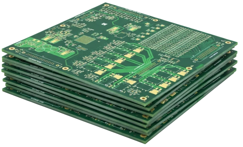
A data-center Ultrasound probe interface PCB is a specialized circuit board designed to bridge high-fidelity medical ultrasound transducers with high-performance computing (HPC) infrastructure. Unlike traditional portable ultrasound carts, these systems are often rack-mounted or integrated into edge-computing servers to process massive amounts of imaging data in real-time using AI algorithms. This PCB must handle two distinct domains: the sensitive analog front-end (AFE) required for the ultrasound probe and the high-speed digital back-end (often PCIe or 100G Ethernet) required to transmit raw data to the data center network.
This guide is written for hardware engineers, procurement leads, and medical device product managers who are scaling from prototype to mass production. You are likely dealing with high channel counts (128 to 256+ channels), strict signal integrity requirements, and the thermal challenges of a server environment. The decision context here is not just about "making it work," but ensuring the board can survive 24/7 operation in a data center rack while maintaining medical-grade reliability.
At APTPCB (APTPCB PCB Factory), we see a growing trend where medical imaging moves from standalone devices to cloud-connected edge nodes. This shift changes the manufacturing requirements significantly. This playbook provides the specifications, risk mitigation strategies, and validation steps necessary to procure these complex boards safely, minimizing the risk of costly respins or field failures.
When to use data-center Ultrasound probe interface PCB (and when a standard approach is better)
Determining whether you need a data-center grade interface or a standard medical PCB is the first step in cost control and design optimization.
Use a data-center Ultrasound probe interface PCB when:
- AI Processing is Centralized: Your system offloads raw RF data to a server rack for image reconstruction and AI diagnostics, requiring massive bandwidth (e.g., PCIe Gen 4/5 interfaces).
- Channel Density is Extreme: You are designing for 256+ channels on a single board, requiring High Density Interconnect (HDI) technology to route signals without crosstalk.
- Continuous Operation is Required: The equipment operates 24/7 in a server room environment, necessitating materials with high thermal reliability (High Tg) and robust thermal management strategies.
- Form Factor is Rack-Mount: The PCB must fit into standard server chassis (e.g., OCP or standard 1U/2U blades), requiring specific mechanical tolerances and airflow considerations.
Stick to a standard Ultrasound probe interface PCB when:
- Processing is Local: The image reconstruction happens on the cart or handheld device itself.
- Battery Power is Primary: Low power consumption is more critical than massive data throughput.
- Standard Connectivity: You only need USB or standard video output, rather than high-speed server interconnects.
- Cost Sensitivity: The project budget cannot support the advanced materials (like Rogers or Megtron) typically required for data-center signal speeds.
data-center Ultrasound probe interface PCB specifications (materials, stackup, tolerances)
Defining the correct specifications upfront prevents ambiguity during the quoting process. These boards are hybrids, mixing sensitive analog signals with aggressive digital interfaces.
- Base Material Selection:
- Hybrid Stackup: Often requires a mix of high-frequency laminates (e.g., Rogers 4350B or Tachyon 100G) for the high-speed digital lines and standard High-Tg FR4 (Tg > 170°C) for power and control layers to balance cost and performance.
- Dielectric Constant (Dk): Tight tolerance on Dk (±0.05) is required for impedance-controlled lines, especially for the PCIe or optical interfaces connecting to the data center network.
- Layer Count & Stackup:
- Layer Range: Typically 12 to 24 layers.
- Signal Isolation: Dedicated ground planes must separate the Analog Front End (AFE) layers from the high-speed digital layers to prevent digital noise from corrupting the ultrasound signal.
- Symmetry: Strictly symmetrical stackup to prevent warpage during reflow, which is critical for large BGA components.
- Trace Width & Spacing:
- Impedance Control: 85Ω or 100Ω differential pairs for high-speed data; 50Ω single-ended for RF traces.
- Minimum Trace/Space: Often down to 3/3 mil (0.075mm) to accommodate high-pin-count AFEs and FPGAs.
- Via Technology:
- HDI Requirement: Type III or Type IV HDI (stacked microvias) is standard to route high-density BGA packages (0.4mm or 0.5mm pitch).
- Back-drilling: Essential for high-speed signals (>10 Gbps) to remove via stubs that cause signal reflection.
- Surface Finish:
- ENIG or ENEPIG: Electroless Nickel Immersion Gold (ENIG) is preferred for flat pads required by fine-pitch BGAs. ENEPIG is used if wire bonding is present.
- Thermal Management:
- Copper Weight: Inner layers may need 2oz copper for power distribution if the board powers the probe.
- Thermal Vias: Dense arrays of thermal vias under FPGAs and power regulators to transfer heat to internal planes or heatsinks.
- Connector Interfaces:
- Edge Plating: Hard gold plating for edge connectors (if plugging into a backplane).
- Press-Fit Holes: Tight tolerances (+0.05/-0.05mm) for high-density press-fit connectors used in server backplanes.
- Cleanliness & Ionic Contamination:
- Standard: IPC-6012 Class 3 (Medical/High Reliability).
- Cleanliness: < 1.56 µg/cm² NaCl equivalent to prevent electrochemical migration in humid environments.
data-center Ultrasound probe interface PCB manufacturing risks (root causes and prevention)
High-complexity boards carry specific manufacturing risks. Understanding these allows you to audit your supplier effectively.
Risk: Analog-Digital Crosstalk
- Root Cause: Improper layer stackup or insufficient shielding between the sensitive ultrasound receiver lines and the high-speed server interface (PCIe/Ethernet).
- Detection: Signal Integrity (SI) simulation failures or high noise floor in prototype testing.
- Prevention: Use "fence vias" (shielding vias) along sensitive traces; enforce strict separation of analog and digital ground planes with a single connection point (star ground).
Risk: BGA Voiding and Open Joints
- Root Cause: Warpage of the large PCB during reflow or improper stencil design for fine-pitch components.
- Detection: X-Ray inspection (2D/3D) and cross-section analysis.
- Prevention: Use Low-CTE materials to match component expansion; optimize reflow profiles using thermal profiling on a dummy board.
Risk: Impedance Mismatch
- Root Cause: Variation in dielectric thickness during lamination or over-etching of copper traces.
- Detection: Time Domain Reflectometry (TDR) testing on coupons and actual boards.
- Prevention: Specify impedance tolerance of ±5% (instead of standard ±10%); require TDR coupons on every production panel.
Risk: Conductive Anodic Filament (CAF) Growth
- Root Cause: High voltage bias between closely spaced vias in a humid environment, leading to internal shorts.
- Detection: High-voltage insulation resistance testing; accelerated life testing.
- Prevention: Use "CAF-resistant" materials; design via-to-via spacing conservatively where possible.
Risk: Plated Through Hole (PTH) Fatigue
- Root Cause: Thermal cycling in a data center environment (heating up under load, cooling down) causes barrel cracks in vias.
- Detection: Thermal shock testing (-40°C to +125°C) followed by micro-sectioning.
- Prevention: Ensure aspect ratio is below 10:1 for mechanical drills; ensure copper plating thickness in holes meets Class 3 specs (avg 25µm).
Risk: Stub Resonance
- Root Cause: Unused portions of vias acting as antennas at high frequencies (25Gbps+).
- Detection: Signal attenuation at specific frequencies (VNA testing).
- Prevention: Implement controlled depth back-drilling to remove via stubs on high-speed lines.
Risk: Surface Finish Oxidation
- Root Cause: Poor storage or handling of ENIG finish before assembly.
- Detection: "Black pad" syndrome or non-wetting during assembly.
- Prevention: Vacuum packaging with desiccant and humidity indicator cards; strict shelf-life controls.
Risk: Registration Errors
- Root Cause: Material movement during lamination of hybrid materials (FR4 + Rogers).
- Detection: X-ray drill verification; cross-section analysis.
- Prevention: Use pin-lamination techniques and scaling factors optimized for the specific hybrid material combination.
data-center Ultrasound probe interface PCB validation and acceptance (tests and pass criteria)

Validation ensures the manufactured board meets the design intent before it enters the assembly line.
- Objective: Signal Integrity Verification
- Method: TDR (Time Domain Reflectometry) on all impedance-controlled lines (single-ended and differential).
- Acceptance Criteria: Impedance must fall within ±5% or ±10% of the target value as specified in the fabrication drawing. No discontinuities > 2Ω along the trace.
- Objective: Interconnect Reliability
- Method: IST (Interconnect Stress Test) or Thermal Shock (500 cycles).
- Acceptance Criteria: Resistance change < 10% from baseline. No barrel cracks or corner cracks in micro-sections.
- Objective: Dielectric Breakdown Voltage
- Method: Hi-Pot testing between isolated nets (e.g., High Voltage transmit lines vs Low Voltage receive lines).
- Acceptance Criteria: No breakdown or leakage current > 1mA at specified test voltage (often >500V for ultrasound transmit pulses).
- Objective: Cleanliness for Reliability
- Method: Ion Chromatography (IC) test.
- Acceptance Criteria: Ionic contamination < 1.0 µg/cm² NaCl equivalent (stricter than standard IPC).
- Objective: Solderability
- Method: IPC-J-STD-003 solderability test.
- Acceptance Criteria: > 95% coverage of the pad surface with fresh solder.
- Objective: Dimensional Accuracy
- Method: CMM (Coordinate Measuring Machine) inspection.
- Acceptance Criteria: Board outline and mounting hole locations within ±0.1mm tolerance to ensure fit in server chassis.
- Objective: Back-drill Depth Verification
- Method: Micro-sectioning or X-ray depth measurement.
- Acceptance Criteria: Remaining stub length < 0.2mm (or as specified); no damage to internal functional layers.
- Objective: Warpage Control
- Method: Shadow Moiré or laser profilometry.
- Acceptance Criteria: Bow and twist < 0.5% (standard is 0.75%, but 0.5% is needed for large BGAs).
data-center Ultrasound probe interface PCB supplier qualification checklist (RFQ, audit, traceability)
Use this checklist to vet potential partners. A supplier must demonstrate capability in both medical reliability and high-speed data center technologies.
RFQ Inputs (What you must provide)
- Gerber Files (RS-274X): Complete set including all copper, solder mask, silk, and drill files.
- IPC Netlist: Essential for electrical testing verification against the design.
- Fabrication Drawing: Clearly stating IPC Class 3 requirements, material types (by trade name, e.g., "Rogers 4350B"), and stackup details.
- Impedance Table: Listing layer, trace width, spacing, and target impedance for all controlled lines.
- Drill Chart: Distinguishing between plated, non-plated, and back-drilled holes.
- Panelization Requirements: If you have specific assembly rails or fiducial placements for your SMT line.
- Volume & EAU: Estimated Annual Usage to determine pricing tiers and production tooling.
- Special Testing: Explicitly request TDR reports, cleanliness reports, and cross-section samples.
Capability Proof (What they must show)
- Hybrid Lamination Experience: Proven track record of bonding FR4 with High-Frequency materials.
- Back-drilling Capability: Equipment and process controls for depth-controlled drilling.
- HDI Competency: Ability to plate stacked microvias reliably (ask for aspect ratio limits).
- Medical Certification: ISO 13485 certification is mandatory for medical device components.
- Data Center Experience: Familiarity with IPC-6012 Class 3 and server-grade reliability standards.
- In-house Testing: Availability of TDR, VNA, and Ion Chromatography equipment on-site.
Quality System & Traceability
- Material Traceability: Ability to trace every PCB back to the specific laminate lot number.
- Process Control: Automated Optical Inspection (AOI) used after inner layer etching and outer layer etching.
- X-Ray Verification: 100% X-ray for multilayer registration and blind/buried vias.
- NCMR Process: Clear procedure for handling Non-Conforming Material Reports.
- Certificate of Conformance (CoC): Shipped with every batch, certifying compliance with all specs.
- UL Marking: Board must carry a UL 94V-0 flammability rating and manufacturer's UL logo.
Change Control & Delivery
- PCN Policy: Supplier must agree to provide Product Change Notification (PCN) before changing materials or processes.
- Buffer Stock: Willingness to hold finished goods inventory (Kanban) for JIT delivery.
- Packaging: ESD-safe, vacuum-sealed packaging with humidity indicators.
- DFM Support: Engineering team available to review designs before manufacturing starts.
- Lead Time Stability: History of on-time delivery performance.
How to choose data-center Ultrasound probe interface PCB (trade-offs and decision rules)
Engineering is about trade-offs. Here is how to navigate the conflicting demands of cost, performance, and reliability for this specific application.
Material: Pure Rogers vs. Hybrid Stackup
- If you prioritize signal integrity above all else (e.g., 56G PAM4 links): Choose a pure high-frequency material stackup. It is expensive but offers the lowest loss.
- If you prioritize cost optimization: Choose a hybrid stackup (Rogers for signal layers, FR4 for power/ground). This is the standard for most data-center ultrasound interfaces.
Surface Finish: ENIG vs. Immersion Silver
- If you prioritize shelf life and BGA reliability: Choose ENIG. It is the gold standard for medical and server boards.
- If you prioritize signal loss at extremely high frequencies (>20GHz): Immersion Silver has slightly better skin-effect properties but tarnishes easily. Stick to ENIG unless you have a specific RF reason not to.
Via Tech: Through-Hole vs. HDI
- If you prioritize routing density (high channel count): You must use HDI (Microvias). It increases cost but reduces board size and layer count.
- If you prioritize lowest board cost: Stick to through-hole technology, but be prepared for a much larger board footprint and potentially more layers to route signals.
Copper Weight: 1oz vs. 2oz+
- If you prioritize power delivery (driving the probe): Use heavy copper (2oz) on inner power planes.
- If you prioritize fine-line etching (impedance control): Keep signal layers at 0.5oz or 1oz. Etching fine lines on heavy copper is difficult and leads to impedance variations.
Testing: Sample vs. 100%
- If you prioritize zero field failures: Mandate 100% electrical test (flying probe or bed of nails) and 100% TDR on coupons.
- If you prioritize prototype speed: You might skip some advanced reliability testing (like IST) on the first spin, but never skip electrical testing.
data-center Ultrasound probe interface PCB FAQ (cost, lead time, Design for Manufacturability (DFM) files, materials, testing)
Q: What is the typical lead time for a data-center Ultrasound probe interface PCB? A: Standard lead time is 15–20 working days due to the complexity of hybrid lamination and HDI processes. Quick-turn options (7–10 days) are available but carry a significant premium and may limit certain surface finish options.
Q: How does the cost of a data-center Ultrasound probe interface PCB compare to a standard medical PCB? A: Expect costs to be 2x–4x higher than standard medical boards. The drivers are expensive high-frequency materials, HDI drilling steps, back-drilling requirements, and Class 3 inspection overhead.
Q: What files are required for a DFM review of a data-center Ultrasound probe interface PCB? A: Beyond standard Gerbers, you must provide an ODB++ file (preferred) or a detailed stackup drawing specifying material types (e.g., "Rogers 4350B 10mil"). Also, include a drill table defining back-drill depths for specific nets.
Q: Can I use standard FR4 for a data-center Ultrasound probe interface PCB? A: Generally, no. Standard FR4 has too much signal loss (Df) for the high-speed data links (PCIe) and inconsistent dielectric constant (Dk) for precise ultrasound beamforming. High-Tg FR4 can be used for power/ground layers in a hybrid stackup, but not for high-speed signal layers.
Q: What are the acceptance criteria for impedance testing on these boards? A: The industry standard is ±10%, but for data-center interfaces, we recommend specifying ±5% for high-speed differential pairs. This requires tighter process control during etching and lamination.
Q: How do you handle thermal management for data-center Ultrasound probe interface PCB designs? A: We recommend using thermal via arrays under hot components (FPGAs, ADCs) connected to internal ground planes. For extreme heat, metal-core or coin-insertion technologies can be explored, though they add significant cost.
Q: Why is back-drilling necessary for data-center Ultrasound probe interface PCB fabrication? A: Back-drilling removes the unused portion of a plated through-hole (the "stub"). At data center speeds (10Gbps+), these stubs act as antennas, causing signal reflections that can corrupt the data integrity.
Q: What is the best surface finish for Ultrasound probe interface PCB assembly? A: ENIG (Electroless Nickel Immersion Gold) is the best all-around choice. It offers a flat surface for fine-pitch BGAs, excellent shelf life, and reliable wire-bonding capabilities if required (or ENEPIG for extensive wire bonding).
Resources for data-center Ultrasound probe interface PCB (related pages and tools)
- Medical PCB Manufacturing: Explore our specific certifications (ISO 13485) and capabilities for medical-grade reliability.
- Server & Data Center PCB: Understand the unique requirements of high-speed, high-uptime server environments that apply to these interface boards.
- HDI PCB Capabilities: Learn about microvias and high-density interconnects essential for routing high-channel-count ultrasound probes.
- High Frequency PCB Materials: Details on Rogers, Taconic, and other low-loss materials required for signal integrity.
- Turnkey PCB Assembly: How we handle the entire process from bare board fabrication to component sourcing and final assembly.
- Impedance Calculator: A tool to help you estimate trace widths and spacing for your required impedance targets before submitting a design.
Request a quote for data-center Ultrasound probe interface PCB (Design for Manufacturability (DFM) review + pricing)
Ready to move your design into production? At APTPCB, we provide a comprehensive DFM review to catch signal integrity risks and manufacturability issues before you pay a cent.
To get an accurate quote and DFM report, please prepare:
- Gerber Files (RS-274X or ODB++)
- Fabrication Drawing (with stackup and material specs)
- Bill of Materials (BOM) (if assembly is required)
- Testing Requirements (TDR, cleanliness, etc.)
- Estimated Volume
Click here to Request a Quote & DFM Review – Our engineering team will review your files and provide a detailed cost analysis and lead time estimate within 24 hours.
Conclusion (next steps)
Successfully deploying a data-center Ultrasound probe interface PCB requires more than just connecting wires; it demands a deep understanding of hybrid materials, signal integrity, and server-grade reliability. By defining strict specifications for materials and stackups, understanding the manufacturing risks like crosstalk and CAF, and enforcing a rigorous validation plan, you can ensure your system performs flawlessly in the demanding environment of a medical data center. Partnering with a capable manufacturer who understands both the medical and high-performance computing domains is the final piece of the puzzle to scale your innovation safely.