In the high-speed world of electronics manufacturing, the difference between a profitable run and a costly recall often comes down to a single process: defect classification smt. Surface Mount Technology (SMT) lines process thousands of components per hour. Without a robust system to categorize, detect, and rectify errors, yield rates plummet.
At APTPCB (APTPCB PCB Factory), we understand that identifying a defect is only half the battle. The real value lies in classifying it correctly to determine the root cause and prevent recurrence. This guide serves as a comprehensive resource for engineers and procurement managers. It covers everything from IPC standards and critical metrics to selecting the right inspection technology for your specific needs.
Key Takeaways
- Hierarchy Matters: Not all defects are equal; they are generally classified as Critical, Major, or Minor based on functionality and reliability risks.
- Standardization: IPC-A-610 is the global benchmark for defining solder joint criteria and acceptance levels.
- Detection vs. Prevention: Effective classification moves you from simply catching bad boards to tuning the process to prevent them.
- The Role of AOI: Automated Optical Inspection is the backbone of modern classification, but it requires precise programming to avoid false calls.
- Data-Driven Decisions: Metrics like DPMO (Defects Per Million Opportunities) and First Pass Yield are essential for validating your classification strategy.
- Validation: Regular cross-checks between machine data and human verification prevent "escape" defects.
What defect classification smt really means (scope & boundaries)
To manage quality effectively, we must first define the boundaries of defect classification smt. It is not merely a list of bad parts. It is a structured approach to categorizing anomalies based on their impact on the final product's performance, reliability, and compliance.
The Three Tiers of Classification
Most industry standards, including those used at APTPCB, follow a three-tier system derived from IPC guidelines:
Critical Defects:
- Definition: Anomalies that are likely to result in hazardous conditions or catastrophic failure of the device.
- Action: Immediate line stop. Quarantine of the entire batch.
- Examples: Electrical shorts on power lines, missing safety components, or severe contamination affecting insulation.
Major Defects:
- Definition: Anomalies that are likely to result in failure or materially reduce the usability of the product for its intended purpose.
- Action: Rework required. Root cause analysis initiated if the frequency exceeds the threshold.
- Examples: Open circuits, missing components, tombstoning, or solder joint criteria violations (e.g., insufficient wetting).
Minor Defects:
- Definition: Anomalies that do not affect the form, fit, or function of the product but violate cosmetic standards.
- Action: Monitor trends. Rework may be optional depending on the customer's cosmetic requirements (Class 2 vs. Class 3).
- Examples: Slight discoloration, minor flux residue, or component shifting that does not violate electrical clearance.
The Role of IPC Standards
The foundation of defect classification smt is the IPC-A-610 standard ("Acceptability of Electronic Assemblies"). This standard provides the visual criteria for what is acceptable. It divides products into three classes:
- Class 1: General Electronic Products (Consumer electronics).
- Class 2: Dedicated Service Electronic Products (Laptops, communications).
- Class 3: High Performance/Harsh Environment (Aerospace, medical, automotive).
A defect in Class 3 might be acceptable in Class 1. Therefore, classification is always relative to the target application.
defect classification smt metrics that matter (how to evaluate quality)
Once you have defined what constitutes a defect, you need to measure how often they occur. Relying on "gut feeling" is dangerous in manufacturing. You need hard data to drive improvement.
The following table outlines the essential metrics for tracking SMT quality.
| Metric | Why it matters | Typical Range / Factors | How to measure |
|---|---|---|---|
| First Pass Yield (FPY) | Indicates the percentage of boards that pass all inspections without any rework. High FPY means a stable process. | 95% - 99%+ (highly dependent on board complexity). | (Good Units / Total Units Entering Process) × 100 |
| DPMO (Defects Per Million Opportunities) | The standard for comparing quality across different board designs. It normalizes defect rates based on complexity. | < 50 for world-class; < 500 for average. | (Total Defects / (Total Units × Opportunities per Unit)) × 1,000,000 |
| False Call Rate (FCR) | Measures how often the inspection machine (AOI) flags a good part as bad. High FCR causes operator fatigue. | Target < 5000 PPM. High FCR leads to real defects being ignored. | (False Rejects / Total Opportunities) × 1,000,000 |
| Escape Rate | The most dangerous metric: defects that slip through inspection and reach the customer. | Target: 0. Even one escape can damage reputation. | (Defects found by customer / Total Defects) × 100 |
| Slip Rate | Defects found at a later stage (e.g., ICT) that should have been caught at SMT. | Varies. Indicates a gap in the defect classification smt strategy. | (Defects found at ICT / Total SMT Defects) |
Understanding these metrics allows you to audit your Quality System effectively. If your FPY is low but your Escape Rate is zero, your inspection is working, but your process is drifting.
How to choose defect classification smt: selection guidance by scenario (trade-offs)
Choosing the right method for defect classification smt involves trade-offs between speed, cost, and depth of analysis. Not every board requires a 3D X-Ray, but relying solely on manual inspection for high-density boards is a recipe for failure.
Here is how to choose the right inspection mix based on your manufacturing scenario.
Scenario 1: NPI and Prototyping
- Context: Low volume (1-10 boards), fast turnaround, unproven design.
- Recommendation: Manual Visual Inspection (MVI) + First Article Inspection (FAI).
- Trade-off: High labor cost per unit, but zero setup time for machines.
- Why: Programming an AOI for 5 boards takes longer than inspecting them manually. FAI systems verify the BOM and polarity before the run continues.
Scenario 2: High-Volume Consumer Electronics
- Context: Thousands of units, cost-sensitive, standard components (0402, QFP).
- Recommendation: Inline 2D or 3D AOI.
- Trade-off: High initial equipment cost, but extremely low per-unit cost.
- Why: AOI basics dictate that cameras can inspect faster than humans. 3D AOI is preferred to measure solder volume and coplanarity.
- Learn more: AOI Inspection Services.
Scenario 3: BGA and Hidden Joints
- Context: Boards utilizing Ball Grid Arrays (BGAs), QFNs, or CSPs where solder joints are underneath the package.
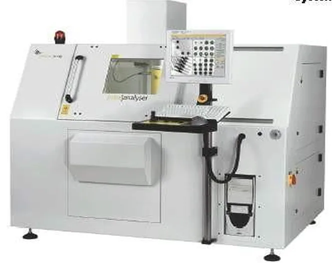
- Recommendation: Automated X-Ray Inspection (AXI).
- Trade-off: Slower cycle time and expensive equipment.
- Why: Optical systems (AOI) cannot see through plastic or silicon. X-Ray is the only non-destructive way to classify voiding and bridging under chips.
Scenario 4: Fine Pitch and Miniaturization
- Context: 0201 or 01005 components, fine-pitch connectors.
- Recommendation: Solder Paste Inspection (SPI) + 3D AOI.
- Trade-off: Adds a step before component placement (SPI).
- Why: 70% of SMT defects originate at the printing stage. SPI catches insufficient paste volume before the part is even placed, saving rework costs.
Scenario 5: High-Reliability (Automotive/Aerospace)
- Context: IPC Class 3 requirements, zero tolerance for failure.
- Recommendation: SPI + 3D AOI + AXI + ICT (In-Circuit Test).
- Trade-off: Highest cost and slowest throughput.
- Why: Redundancy is required. A defect missed by AOI must be caught by electrical testing.
Scenario 6: Legacy or Through-Hole Mix
- Context: SMT boards that also require manual insertion of large connectors or capacitors.
- Recommendation: AOI for SMT + Manual Check for THT.
- Trade-off: Balanced approach.
- Why: AOI machines often struggle with the variable height and shape of hand-soldered through-hole parts.
defect classification smt implementation checkpoints (design to manufacturing)
Implementing a robust defect classification smt strategy starts long before the pick-and-place machine warms up. It begins at the design stage.
Below is a checklist to ensure your product is ready for accurate defect classification.
1. Design for Manufacturing (DFM) Review
- Recommendation: Ensure component footprints match IPC standards.
- Risk: If pads are too small, AOI will flag "insufficient solder" even if the joint is mechanically sound.
- Acceptance: Pass DFM check with no critical errors.
- Resource: DFM Guidelines.
2. Fiducial Marker Placement
- Recommendation: Place at least three global fiducials on the panel rails and local fiducials near fine-pitch parts.
- Risk: Without fiducials, the AOI machine cannot align its coordinate system, leading to massive false calls on position.
- Acceptance: Clear contrast fiducials present in Gerber data.
3. Component Library Standardization
- Recommendation: Use standard package sizes. Avoid mixing metric and imperial codes in BOMs.
- Risk: Mismatched library data causes the machine to look for a resistor that is twice the size of the actual part.
- Acceptance: BOM scrub completed.
4. Stencil Design Verification
- Recommendation: Optimize aperture design for paste release.
- Risk: Poor release leads to bridging. If the defect classification system isn't tuned, it might misidentify bridges as "misalignment."
- Acceptance: SPI volume data within 80%-120% target.
5. Reflow Profile Tuning
- Recommendation: Use a thermal profiler to ensure all joints reach liquidus.
- Risk: Cold solder joints are notoriously difficult for 2D AOI to detect.
- Acceptance: Profile falls within paste manufacturer specs.
6. Inspection Threshold Setup
- Recommendation: Run a "Golden Board" (known good board) to teach the AOI.
- Risk: Setting tolerances too tight results in high false calls; too loose results in escapes.
- Acceptance: False call rate < 5000 PPM during trial run.
7. Operator Training
- Recommendation: Train operators on solder joint criteria and how to verify AOI flags.
- Risk: Operators may habitually hit "Accept" on false calls, eventually accepting a real defect.
- Acceptance: Operators certified to IPC-A-610.
8. Data Loop Feedback
- Recommendation: Feed AOI data back to the printer and mounter.
- Risk: Fixing defects without fixing the source ensures they will happen again.
- Acceptance: Process capability (Cpk) improves over time.
defect classification smt common mistakes (and the correct approach)
Even with high-end equipment, manufacturers often struggle with defect classification smt. Here are the most common pitfalls and how APTPCB avoids them.
1. Ignoring the "False Call" Fatigue
- Mistake: Engineers set AOI sensitivity to maximum to catch everything. The machine flags 50 errors per board, 49 of which are false.
- Consequence: The operator stops looking closely and mass-accepts the list, missing the 1 real defect.
- Correction: Tune the lighting and algorithms to reduce false calls to a manageable level.
2. Relying Solely on Electrical Test (ICT)
- Mistake: Assuming that if a board passes the electrical test, it is perfect.
- Consequence: A "near-open" joint (barely touching) will pass electrical test but fail in the field after vibration.
- Correction: Visual inspection (AOI/X-Ray) is mandatory to verify structural integrity, not just connectivity.
3. Inconsistent Defect Naming
- Mistake: One operator calls it "insufficient solder," another calls it "open."
- Consequence: Data analysis becomes impossible. You cannot track the root cause if the data is messy.
- Correction: Standardize the defect dictionary based on IPC terms.
4. Skipping SPI (Solder Paste Inspection)
- Mistake: Viewing SPI as an unnecessary cost.
- Consequence: Defects are found at the end of the line (post-reflow), requiring expensive rework with soldering irons.
- Correction: Catch paste issues immediately after printing. Wiping a board clean is cheaper than desoldering components.
5. Neglecting Shadowing Effects
- Mistake: Placing tall components (electrolytic caps) right next to small resistors.
- Consequence: The tall component blocks the AOI camera's view or casts a shadow, making inspection impossible.
- Correction: Address component layout during the DFM phase.
6. Lack of Calibration
- Mistake: Failing to calibrate inspection equipment regularly.
- Consequence: Measurement drift leads to inaccurate classification of component shifts or skew.
- Correction: Scheduled maintenance and calibration using certified artifacts.
defect classification smt FAQ (cost, lead time, Design for Manufacturing (DFM) files, stackup, Measures how often the inspection machine (AOI) inspection, X-ray inspection)
Q: What is the difference between AOI and X-Ray inspection? A: AOI uses cameras and light to inspect visible features like component placement and visible solder fillets. X-Ray penetrates the board to inspect hidden features, such as BGA balls or voiding inside a solder joint.
Q: How do you calculate DPMO for a PCB? A: DPMO = (Total Number of Defects / (Total Number of Units × Total Opportunities per Unit)) × 1,000,000. An "opportunity" is any chance for a defect, such as a component placement or a solder joint.
Q: What is a "Champagne Void"? A: This is a specific type of void found in BGAs where the void is located at the interface between the solder ball and the package pad. It is a critical defect often caused by plating issues.
Q: Can defect classification be fully automated? A: While machines (AOI/SPI) do the heavy lifting of detection, final classification often requires human verification to rule out false calls. AI-powered AOI is reducing the need for human intervention, but human oversight remains crucial for Class 3 products.
Q: What is the difference between IPC Class 2 and Class 3 regarding defects? A: Class 2 allows for some imperfections (e.g., 50% vertical fill in a through-hole barrel). Class 3 is stricter (e.g., 75% vertical fill) because the product must function without interruption in harsh environments.
Q: Why is "Head-in-Pillow" difficult to detect? A: Head-in-Pillow (HiP) occurs when a BGA ball rests on the paste but doesn't coalesce. It often passes DC electrical tests but fails at high frequencies or under thermal stress. X-Ray is usually required to detect the subtle shape difference.
Q: Does APTPCB provide inspection reports? A: Yes. We can provide AOI, X-Ray, and FAI reports upon request to validate that the defect classification smt process was followed.
defect classification smt glossary (key terms)
| Term | Definition |
|---|---|
| AOI | Automated Optical Inspection. Uses cameras to scan PCBs for catastrophic failures and quality defects. |
| Bridging | A defect where solder connects two or more adjacent pads that should be electrically isolated (Short Circuit). |
| Coplanarity | The condition where all leads of a component lie on the same geometric plane. Lack of coplanarity leads to open joints. |
| DPMO | Defects Per Million Opportunities. A standard metric for process quality. |
| Fiducial | A copper marker on the PCB used by assembly machines as a reference point for alignment. |
| Head-in-Pillow | A BGA defect where the solder ball rests on the pad paste but does not fully merge. |
| IPC-A-610 | The industry standard for the acceptability of electronic assemblies. |
| Manhattan Effect | Also known as Tombstoning. A component stands up on one end due to uneven wetting forces during reflow. |
| Skew | A defect where the component is rotated or shifted off its target pad but is still electrically connected. |
| Solder Beading | Large solder balls that form alongside chip components, often due to excess paste. |
| SPI | Solder Paste Inspection. Measures the volume, height, and area of solder paste deposits. |
| Tombstoning | See Manhattan Effect. |
| Voiding | Empty spaces or air pockets within a solder joint. Acceptable up to a certain percentage (usually 25%). |
| Wetting | The ability of molten solder to spread and bond with the metal surface of the pad and component lead. |
Conclusion (next steps)
Mastering defect classification smt is not just about buying the most expensive inspection machine. It is about integrating design, process control, and validation into a cohesive system. By understanding the hierarchy of defects, monitoring metrics like DPMO, and selecting the right inspection tools for your specific scenario, you can drastically reduce risk and improve yield.
At APTPCB, we employ a multi-stage inspection strategy—including SPI, 3D AOI, and X-Ray—to ensure every board meets your specified IPC class.
Ready to move your design into production? When submitting your data for a DFM review or quote, please provide:
- Gerber Files: Including paste, mask, and silk layers.
- BOM (Bill of Materials): With manufacturer part numbers.
- Assembly Drawings: Indicating polarity and special instructions.
- Test Requirements: Specify if you need ICT, FCT, or specific X-Ray coverage.
- IPC Class: Specify if you require Class 2 or Class 3 inspection standards.
Ensuring these details are clear from day one allows us to calibrate our defect classification smt protocols to your exact needs, delivering a product you can trust.