- PCB layout DFM is strongest when it is treated as a design review before fabrication, not as a universal table of geometry limits.
- The real question before fabrication is whether the board intent is clear enough for fabrication, assembly, and test teams to work without guessing.
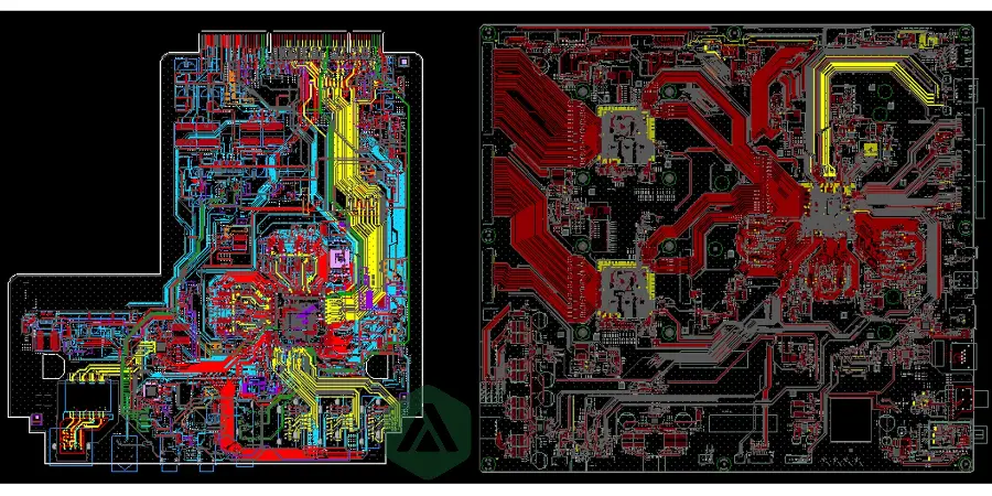
- A layout can pass CAD checks and still stall at factory review if stackup details, package choices, manufacturing notes, or test expectations remain vague.
Quick Answer DFM guidelines for PCB layout should be used to confirm five things before a board moves forward: the board type is clear, the stackup is defined clearly, package and footprint decisions are reviewable, the manufacturing file set is complete, and downstream assembly or test assumptions are visible early.
Table of Contents
- What DFM guidelines for PCB layout really mean
- What should be reviewed first
- How DFM, DFA, and DFT fit together
- Where package and footprint review enters
- What belongs in the manufacturing package
- When a layout should pause for engineering review
- Next steps with APTPCB
- FAQ
- Public references
What DFM guidelines for PCB layout really mean
Here, DFM guidelines for PCB layout do not mean a generic promise that the board is already easy to manufacture. They mean a structured review of whether the layout package is clear enough for the next manufacturing decisions.
That review usually sits between schematic completion and fabrication release. It asks whether the board package explains:
- what construction family the design belongs to
- which stackup assumptions are fixed and which are still conditional
- whether package, footprint, and orientation decisions are documented clearly
- how fabrication and assembly teams should read the data set
- what test or validation path is expected after the build
This is why a strong DFM article should stay focused on manufacturing clarity. It should not pretend that one checklist alone proves volume readiness, long-term reliability, or final validation completion.
What should be reviewed first
Before anyone debates isolated layout rules, review the board at the package level.
| Review area | What to confirm | Why it matters |
|---|---|---|
| Board type | Is the board still baseline rigid, or has it already moved into HDI, hybrid, high-layer, rigid-flex, or another special build type? | The manufacturing route changes before individual rule details matter |
| Stackup intent | Does the layer structure describe the real build plan, not only a routing preference? | Fabrication and impedance planning depend on the same stackup story |
| Package clarity | Are package identity, footprint choice, pin-1, polarity, and documentation marks reviewed cleanly? | Assembly and inspection risk often begins here |
| Data completeness | Does the manufacturing package include the fabrication data, notes, stackup context, and assembly-supporting inputs? | Exported image data alone does not explain board intent |
| Testing approach | Is the expected first-build, inspection, and test path visible? | Test access and handoff decisions become harder when introduced late |
The main DFM mistake is to start with isolated geometry concerns while the higher-level manufacturing picture is still unstable. If the board type or manufacturing file set is still drifting, detailed rule cleanup does not solve the real risk.
How DFM, DFA, and DFT fit together
PCB layout reviews are stronger when DFM, DFA, and DFT are treated as linked front-end gates.
DFM
This is the fabrication-facing gate. It checks whether the board structure, stackup direction, edge definition, and fabrication notes are coherent enough for factory review.
DFA
This is the assembly-facing gate. It checks whether package choices, orientation, polarity marking, placement logic, and handling assumptions are reviewable by the assembly team.
DFT
This is the test-facing gate. It checks whether the board leaves room for the intended inspection or electrical test path, and whether the build package makes that path visible early enough.
None of these gates should be written as proof that the board is already qualified or ready for volume release. They are front-end review stages that reduce ambiguity before the build moves forward.
Where package and footprint review enters
Many layout review failures start in the package library rather than in the copper pattern.
The review should confirm:
- the package family naming is clear
- the footprint object matches the intended part identity
- origin, pin-1, polarity, and reference-marking logic are reviewable
- special assembly-sensitive packages are not relying on silent assumptions
- any exact geometry claims still belong to stronger package-owner sources, not to generic blog wording
One of the most expensive layout-side mistakes hides inside the CAD library default for large thermal pads. Many CAD tools, or rushed engineers, leave the Paste mask 1:1 ratio on a QFN or other BTC center thermal pad exactly equal to the copper area. In the 3D view, nothing looks wrong. In SMT, it is a trap. That giant stencil opening prints an excessive solder volume directly under the middle of the package. During reflow, the center pad turns into a heavy molten solder pool and the package begins to lift. The result is Component Float or skew at the exact moment the outer fine-pitch leads are supposed to wet and collapse. Instead of a stable solder joint, the device rides upward on the center pad and the perimeter pins lose contact. What leaves the oven is not a minor process deviation. It is a package with effectively 100% Open joints around the signal pins. This is why layout DFM cannot stop at trace and space checks. If paste reduction and window-pane logic are not locked before release, clean routing will still manufacture scrap.
This is one reason PCB Design Review Checklist belongs in the same review flow. The article should not act like a universal footprint rulebook. It should explain how package review is folded into the larger pre-release manufacturing review.
What belongs in the manufacturing package
A manufacturable layout package is more than a set of artwork files.
At minimum, the manufacturing package should make the following items readable:
- fabrication data package
- stackup or construction direction
- board outline and route intent
- assembly-supporting inputs such as placement or orientation context
- BOM or part-identity context where required for review
- notes about controlled structures, special build types, or unresolved items
- test or validation expectations for the first build
This boundary matters because no single export format should be treated as automatic proof that fabrication, assembly, and test all have enough context. A board package becomes stronger when these inputs are aligned, not when the team assumes one file set explains everything.
A common DFM failure chain starts when the layout passes CAD checks but the release package still leaves one key intent unstated: the stackup note does not match the routing posture, the package-library revision is not frozen, or assembly-supporting orientation context is missing from the handoff set. Fabrication, CAM, or SMT review then fills the gap with a workable assumption so the build can move. That assumption survives longer than it should because the exports look complete. The mismatch is discovered only when assembly setup, inspection, or first-build debug shows that the package was manufacturable only under a different interpretation, which turns a quiet documentation gap into rework and release delay.
For stackup-specific planning, the companion page is PCB Stackup Design. For service-side routing, the commercial support path is PCB Stack-Up.
When a layout should pause for engineering review
Pause the release when the package still leaves the factory guessing.
Common pause points include:
- the board is still ambiguous between baseline rigid and a special build type
- the stackup description and the actual routing intent do not match
- package and footprint review is incomplete for assembly-sensitive devices
- the fabrication package is exportable but not clearly documented
- assembly or test assumptions appear only after layout is already frozen
- unresolved exceptions are known internally but missing from the release notes
These are usually better indicators of risk than a long public checklist of isolated dimensions. A practical DFM review focuses on missing clarity and missing context first.
Next steps with APTPCB
If the board has already reached the point where fabrication, assembly, or test teams need to read the same release package, start with the broader PCB Design for Manufacturing Guide.
If the main uncertainty is stackup definition, branch selection, or controlled-structure planning, continue with PCB Stackup Design.
If the layout is ready for a manufacturing-side review, send the fabrication package, stackup intent, board-edge notes, BOM context, placement or orientation context, and test expectations through the quote page. APTPCB's engineering team can review whether the main gap sits in board-type definition, package review, file completeness, release-package alignment, or test-planning clarity.
Next steps with APTPCB
If you are about to release a dense PCB layout for production and still have doubts about whether the CAD package library really matches the assembly process, whether the stackup can hold the intended impedance, or whether test coverage is leaving blind spots, do not wait for fabrication and SMT to discover the mismatch for you. This is where apparently clean data packages still hide paste-opening traps, stackup tolerance risk, and assembly assumptions that only become visible after money has already been committed to physical build.
Send the Gerber, ODB++, or IPC-2581 package, full BOM, and stackup intent to sales@aptpcb.com or through the quote page.
APTPCB's CAM and NPI engineering team will return a Layout DFM & Manufacturability Blind-spot Review within 24 hours. We will identify paste-opening traps in package libraries, verify stackup tolerance assumptions, and expose the manufacturing blind spots most likely to reduce First-Pass Yield before your tooling, solder mask, and build cost are turned into physical scrap.
FAQ
Are DFM guidelines only about fabrication limits?
No. Fabrication rules matter, but this topic is stronger as a release-clarity review that also checks package review, documentation, and downstream handoff.
Can DFM alone prove the board is ready for mass production?
No. DFM helps structure the review, but it does not replace later build evidence, inspection results, or program-specific validation.
Should a DFM article publish universal drill, annular ring, or spacing rules?
Not by default. Those values depend on the board type, stackup, copper, build method, and stronger source scope than a generic DFM article should assume.
What usually creates review delays first?
Unclear stackup definition, incomplete manufacturing notes, package-library ambiguity, and late test assumptions usually create delays before isolated rule details do.
Public references
PCB Design for Manufacturing Guide Pillar page for DFM review and manufacturing preparation.
PCB Design Review Checklist Companion article for staged review before fabrication, assembly, and test handoff.
PCB Stackup Design Companion article for board-type and stackup planning.
PCB Stack-Up Support-page context for stackup structure and manufacturing discussion.
DFM Guidelines Support-page context for manufacturing-side review intake.
Author and review information
- Author: APTPCB layout DFM content team
- Technical review: fabrication intake, CAM, and pre-release review team
- Last updated: 2026-05-15