Digital Radiography PCB quick answer (30 seconds)
Digital Radiography (DR) PCBs act as the control and readout backbone for flat-panel detectors (FPDs), requiring strict adherence to signal integrity and medical safety standards. Unlike standard electronics, these boards must withstand cumulative radiation exposure and manage high-speed image data transfer without introducing noise artifacts.
- Radiation Hardness: Standard FR-4 may degrade (discolor or become brittle) under high-energy X-rays; use high-Tg materials or specific radiation-resistant laminates for long-term reliability.
- Noise Floor: The PCB layout must separate analog sensor signals from high-speed digital logic to prevent image artifacts; a split ground plane strategy is often required.
- Safety Compliance: Designs must meet IEC 60601-1 standards, specifically requiring 2 MOOP PCB (Means of Operator Protection) spacing for isolation barriers.
- High-Density Interconnects: Readout ICs (ROICs) often require fine-pitch BGA or Chip-on-Flex (COF) connections, necessitating HDI technology with laser-drilled microvias.
- Thermal Management: Detectors generate heat which increases thermal noise; the PCB must integrate thermal vias or metal cores to dissipate heat away from the sensor array.
- Data Throughput: Supports high-bandwidth interfaces (GigE, USB 3.0, or fiber optics) to transmit high-resolution images instantly.
When Digital Radiography PCB applies (and when it doesn’t)
Identifying the correct application ensures that the cost and complexity of medical-grade manufacturing are justified.
Applies to:
- Medical X-ray Detectors: Static and dynamic flat-panel detectors for chest, dental, and mammography imaging.
- Industrial NDT (Non-Destructive Testing): High-energy X-ray inspection systems for pipeline or aerospace component analysis.
- Veterinary Imaging Systems: Portable DR panels requiring ruggedized, shock-resistant PCB assemblies.
- Security Screening: Baggage scanners using linear diode arrays requiring long, synchronized readout boards.
- High-Resolution Optical Imaging: Similar layout principles apply to a Digital Microscope PCB where sensor noise must be minimized.
Does NOT apply to:
- MRI Control Systems: These require non-magnetic materials and different RF shielding strategies, not just X-ray hardness.
- Standard Consumer Cameras: While they use image sensors, they lack the high-voltage isolation and radiation durability requirements.
- Low-Frequency Analog Devices: DR systems operate at high speeds; standard analog rules do not cover the LVDS/DDR routing needs of digital radiography.
Digital Radiography PCB rules and specifications (key parameters and limits)
APTPCB (APTPCB PCB Factory) recommends adhering to strict parameter limits to ensure the final board passes medical certification and functions correctly in a radiation environment.
| Rule | Recommended Value/Range | Why it matters | How to verify | If ignored |
|---|---|---|---|---|
| Dielectric Material (Tg) | Tg > 170°C (High Tg FR-4 or Polyimide) | Resists thermal stress and radiation-induced degradation. | DSC (Differential Scanning Calorimetry) test. | Board delamination or warping during operation. |
| Trace Impedance | 90Ω / 100Ω ±10% (Differential) | Critical for LVDS lines carrying image data from ROICs to the processor. | TDR (Time Domain Reflectometry) impedance testing. | Data packet loss, image artifacts, or sync errors. |
| Isolation Distance (2 MOOP) | ≥ 4mm creepage / 2.5mm clearance (varies by voltage) | Ensures operator safety per IEC 60601-1 (2 MOOP PCB requirement). | CAD rule check & Hi-Pot testing. | Failed safety certification; shock hazard. |
| Copper Weight | 1 oz to 2 oz (Inner/Outer) | Sufficient for power distribution without excessive etching undercut. | Microsection analysis. | Voltage drops causing sensor calibration errors. |
| Surface Finish | ENIG or ENEPIG | Provides a flat surface for fine-pitch BGAs and wire bonding. | X-ray fluorescence (XRF) thickness measurement. | Poor solder joints on readout chips; open circuits. |
| Via Structure | Blind/Buried Vias (HDI) | Essential for routing thousands of pixel signals in compact detectors. | Cross-sectioning. | Impossible to route high-resolution arrays; increased board size. |
| Cleanliness (Ionic) | < 1.56 µg/cm² NaCl equivalent | Ionic residues can cause electrochemical migration under high voltage. | ROSE testing (Resistivity of Solvent Extract). | Dendrite growth causing shorts in high-voltage bias lines. |
| Solder Mask | LDI (Laser Direct Imaging) Green/Blue | High precision for fine-pitch pads; specific colors may aid automated optical inspection. | Visual inspection / Adhesion test. | Solder bridging on fine-pitch ROIC pads. |
| Aspect Ratio | 8:1 to 10:1 | Ensures reliable plating in through-holes for thick boards. | Microsectioning. | Barrel cracks or open vias during thermal cycling. |
| Layer Count | 8 to 16 Layers | Required to segregate analog, digital, and power planes effectively. | Stackup verification. | High noise floor; poor image quality. |
Digital Radiography PCB implementation steps (process checkpoints)
Successful production requires a synchronized workflow between design and manufacturing.
- Schematic Partitioning:
- Action: Group components by function (High Voltage Bias, Analog Readout, Digital Processing, Power).
- Check: Ensure no digital return currents cross analog reference planes.
- Stackup Definition:
- Action: Define layer stack with APTPCB engineers to balance impedance and signal isolation. Place ground planes adjacent to signal layers.
- Check: Verify material availability (e.g., Isola 370HR or equivalent High Tg).
- Layout and Routing:
- Action: Route differential pairs first. Apply 2 MOOP PCB spacing rules to high-voltage sections.
- Check: Run DRC (Design Rule Check) for creepage and clearance violations.
- DFM Review:
- Action: Submit Gerbers for analysis of annular rings, drill aspect ratios, and fine-pitch suitability.
- Check: Confirm minimum trace/space capabilities (e.g., 3/3 mil for HDI).
- Fabrication (Lamination & Drilling):
- Action: Execute controlled depth drilling for blind vias. Use laser drilling for microvias if HDI is specified.
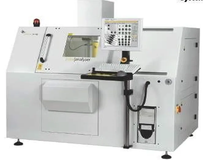
- Check: X-ray verify drill alignment to inner layers.
- Surface Finishing:
- Action: Apply ENIG for flat pads.
- Check: Measure gold/nickel thickness to prevent "black pad" syndrome.
- Assembly (PCBA):
- Action: Mount BGA/CSP components using precision pick-and-place. Reflow with a profile optimized for the specific thermal mass.
- Check: 100% Automated Optical Inspection (AOI) to detect skew or tombstoning.
- Electrical & Functional Testing:
- Action: Perform ICT (In-Circuit Test) and functional image capture tests.
- Check: Verify noise floor levels are within sensor specifications.
Digital Radiography PCB troubleshooting (failure modes and fixes)
When a Digital Radiography PCB fails, the symptoms often appear in the image quality or communication stability.
Symptom: Horizontal Line Artifacts in Image
- Cause: Power supply ripple or noise coupling from digital lines into the analog readout traces.
- Check: Probe power rails with an oscilloscope; review layout for digital traces crossing analog splits.
- Fix: Add decoupling capacitors close to ROIC power pins; redesign stackup to improve shielding.
Symptom: Intermittent Connection / Image Dropouts
- Cause: Fractured solder joints on BGAs due to mechanical flexing (common in portable detectors) or thermal expansion mismatch.
- Check: Perform X-ray Inspection on BGA components; check for "head-in-pillow" defects.
- Fix: Use underfill for BGAs to improve mechanical strength; switch to flexible or rigid-flex materials if mechanical stress is high.
Symptom: High Voltage Arcing / Short Circuit
- Cause: Insufficient creepage distance between the HV bias line (often >100V) and low-voltage logic, or board contamination.
- Check: Inspect for carbonization tracks; verify cleanliness levels.
- Fix: Increase isolation spacing (2 MOOP); apply conformal coating to high-voltage areas.
Symptom: "Salt and Pepper" Noise Increasing Over Time
- Cause: Radiation damage to the PCB dielectric or active components, leading to increased leakage current.
- Check: Compare current noise floor with baseline data from when the board was new.
- Fix: This is often a lifespan issue. Use radiation-hardened components and materials for the next revision.
Symptom: Communication Failure (GigE/USB)
- Cause: Impedance mismatch on differential pairs causing signal reflection.
- Check: TDR measurement of the transmission lines.
- Fix: Adjust trace width/spacing in the layout to match the stackup dielectric constant.
How to choose Digital Radiography PCB (design decisions and trade-offs)
Selecting the right architecture depends on the detector type (Static vs. Dynamic) and portability.
1. Rigid vs. Rigid-Flex
- Rigid PCB: Best for fixed detectors (e.g., wall stands). Lower cost, higher layer count potential.
- Rigid-Flex PCB: Essential for portable detectors where the readout electronics must fold behind the sensor panel to minimize the "dead zone" at the edges. This reduces the overall device footprint but increases manufacturing cost and complexity.
2. Material Selection: Standard High-Tg vs. Specialized Low-Loss
- Standard High-Tg FR-4: Sufficient for most static X-ray detectors where data rates are moderate.
- Low-Loss Material (e.g., Rogers/Megtron): Required for dynamic detectors (fluoroscopy/CT) transmitting high-frame-rate video data (10Gbps+). Reduces signal attenuation but costs significantly more.
3. Integration Level: Chip-on-Board (COB) vs. SMT
- SMT (Surface Mount): Standard packaged ICs. Easier to repair and assemble.
- COB (Chip on Board): Bare die wire-bonded directly to the PCB. Used when space is extremely limited (e.g., dental sensors). Requires gold surface finish and cleanroom assembly.
4. Safety Standard: 1 MOOP vs. 2 MOOP PCB
- 1 MOOP: Acceptable if the device has a separate protective earth ground and is not in direct patient contact.
- 2 MOOP: Mandatory for patient-contact parts or devices without protective earth. Always design for 2 MOOP if the classification is ambiguous to future-proof the product.
Digital Radiography PCB FAQ (cost, lead time, common defects, acceptance criteria, Design for Manufacturability (DFM) files)
Q: What is the typical lead time for a Digital Radiography PCB prototype? A: Standard lead time is 8–12 days for complex HDI boards. Expedited services can reduce this to 5–7 days, depending on layer count and material availability.
Q: How does the cost of a Digital Radiography PCB compare to a standard board? A: Expect costs to be 2–3x higher due to High-Tg materials, HDI laser drilling, strict impedance control, and Class 3 inspection requirements.
Q: What files are required for a DFM review? A: Send Gerber files (RS-274X), NC Drill files, IPC-356 netlist (for electrical test verification), and a detailed stackup drawing specifying impedance requirements.
Q: Can you manufacture PCBs for Digital Microscope applications? A: Yes, a Digital Microscope PCB shares many requirements with DR boards, including high-density sensor interconnects and low-noise signal processing.
Q: What are the acceptance criteria for these PCBs? A: We typically follow IPC-6012 Class 3 (High Reliability Medical/Aerospace). This mandates tighter tolerances on annular rings, plating thickness, and visual defects.
Q: Do I need specific testing for 2 MOOP compliance? A: The PCB fabrication must ensure physical spacing (creepage/clearance). The final assembly should undergo Hi-Pot (Dielectric Withstand) testing to verify the isolation barrier holds under voltage.
Q: How do you handle the high voltage bias for the sensor? A: We route HV traces on internal layers with increased clearance or use slots (milled air gaps) on the PCB to physically prevent arcing.
Resources for Digital Radiography PCB (related pages and tools)
- Medical PCB Manufacturing: Overview of capabilities for healthcare electronics.
- HDI PCB Technology: Details on microvias and fine-pitch routing essential for detector arrays.
- DFM Guidelines: Design rules to ensure your board is manufacturable without revision spins.
Digital Radiography PCB glossary (key terms)
| Term | Definition |
|---|---|
| FPD (Flat Panel Detector) | The core component of digital radiography, consisting of a scintillator and a TFT/photodiode array. |
| Scintillator | A material that converts X-rays into visible light, which is then detected by the sensor. |
| ROIC (Readout IC) | Integrated circuits that amplify and digitize the signals from the sensor pixels. |
| 2 MOOP | Two Means of Operator Protection. A safety standard requiring double insulation or reinforced isolation. |
| TFT (Thin Film Transistor) | The switch at each pixel that allows the charge to be read out. |
| DQE (Detective Quantum Efficiency) | A measure of the imaging system's efficiency in converting X-ray input to a useful image signal. |
| Creepage Distance | The shortest path between two conductive parts measured along the surface of the insulation. |
| Clearance | The shortest distance between two conductive parts measured through air. |
| Dark Current | The residual electric current flowing in the sensor when no radiation is present; contributes to noise. |
| Ghosting | An image artifact where a previous exposure remains visible in subsequent images due to incomplete charge transfer. |
Request a quote for Digital Radiography PCB
APTPCB specializes in high-reliability medical electronics. For a precise quote and DFM review, please provide your Gerber files, stackup specifications, and estimated annual volume.
Checklist for Quote Request:
- Gerber Files: RS-274X or ODB++ format.
- Fabrication Drawing: Specify Class 3 requirements, material Tg, and surface finish.
- Impedance Table: List target impedances for LVDS/USB lines.
- Volume: Prototype quantity vs. mass production targets.
Conclusion (next steps)
A successful Digital Radiography PCB project relies on balancing signal integrity with robust mechanical and safety design. By selecting the right High-Tg materials, enforcing 2 MOOP PCB isolation rules, and utilizing HDI techniques for fine-pitch sensors, you ensure your medical imaging device delivers clear, reliable diagnostics. APTPCB is ready to support your engineering team from initial layout review through to mass production of medical-grade assemblies.