Definition, scope, and who this guide is for
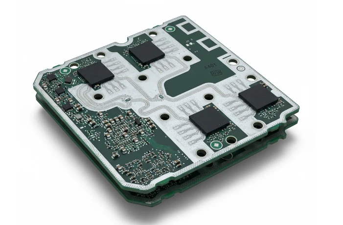
A Distributed Antenna System (DAS) is a network of spatially separated antenna nodes connected to a common source via a transport medium that provides wireless service within a geographic area or structure. In the context of hardware procurement and PCB manufacturing, "Distributed Antenna System" refers specifically to the fabrication and assembly of the printed circuit boards that drive the Master Units, Expansion Units, and Remote Radio Units (RRUs). These boards are the physical backbone of indoor and outdoor coverage solutions, requiring a fusion of high-speed digital processing and high-frequency RF transmission capabilities.
This guide is written for RF engineers, hardware architects, and procurement leads responsible for sourcing PCBs for DAS infrastructure. It moves beyond general system architecture to focus on the manufacturability, material selection, and quality assurance of the underlying hardware. Whether you are deploying a passive DAS for a small office or an active digital DAS for a stadium, the reliability of the system hinges on the integrity of the PCB substrate, the precision of the etching, and the stability of the signal path.
Readers will gain a structured approach to defining specifications that minimize Passive Intermodulation (PIM), identifying manufacturing risks before they become field failures, and validating suppliers like APTPCB (APTPCB PCB Factory) who specialize in communication infrastructure. This playbook provides the technical depth needed to transition from a prototype design to volume production without compromising signal integrity or blowing the budget on unnecessary material costs.
When to use Distributed Antenna System (and when a standard approach is better)
Understanding the physical constraints of your coverage area is the first step in determining if a Distributed Antenna System is the correct hardware solution. While standard macro cells or small cells offer simpler deployment models, they often fail in complex RF environments where signal penetration and capacity are paramount.
Use a Distributed Antenna System when:
- High-Density Environments: You are designing for stadiums, airports, or convention centers where thousands of users access the network simultaneously, requiring the granular capacity management that only a DAS can provide.
- Signal Shadowing: The target environment includes thick concrete walls, underground tunnels (subways), or metal-heavy industrial zones where external macro signals cannot penetrate.
- Multi-Carrier Support: The hardware must support multiple frequency bands and carriers on a single infrastructure, necessitating broadband Antenna System PCB designs that maintain linearity across a wide spectrum.
- 5G/6G Implementation: You are deploying high-frequency 5G Antenna PCB or future 6G Antenna PCB solutions where signal attenuation is high, requiring remote units to be closer to the user equipment.
- Precise RF Containment: The application requires strictly contained signals (e.g., secure government facilities or hospitals) to prevent interference with outside networks.
Stick to Standard Small Cells or Macro Towers when:
- Low Capacity Requirements: The user density is low, and simple coverage extension is the only goal; a repeater or a few Wi-Fi access points may suffice.
- Single Carrier/Band: The deployment is dedicated to a specific narrow band where a dedicated small cell is more cost-effective than a broadband DAS.
- Budget Constraints: The upfront infrastructure cost of fiber backbones and complex head-end equipment is prohibitive compared to standalone access points.
- Rapid Deployment: You need a solution installed in days rather than months; DAS requires significant cabling and architectural integration.
Distributed Antenna System specifications (materials, stackup, tolerances)
Defining the correct specifications upfront is critical for DAS performance, particularly regarding PIM and impedance control. Below are the key parameters to define in your fabrication drawing and documentation package.
- Base Material Selection: Specify high-frequency laminates for RF layers (e.g., Rogers RO4350B, RO4003C, or Taconic RF-35) combined with high-Tg FR4 for digital control layers in a hybrid stackup.
- Dielectric Constant (Dk) Tolerance: Require Dk tolerances of ±0.05 or tighter for the RF layers to ensure consistent phase velocity and impedance matching across the Antenna System PCB.
- Dissipation Factor (Df): Specify ultra-low loss materials (Df < 0.003 @ 10GHz) for signal paths to minimize insertion loss, especially for long traces in Master Units.
- Copper Surface Roughness: Explicitly request "Very Low Profile" (VLP) or "Reverse Treated Foil" (RTF) copper to reduce conductor loss and mitigate PIM effects caused by the skin effect at high frequencies.
- Impedance Control: Define impedance targets (usually 50Ω single-ended, 100Ω differential) with a strict tolerance of ±5% rather than the standard ±10%, as reflections in a DAS can severely degrade throughput.
- Passive Intermodulation (PIM) Rating: Specify a PIM rating for the bare board (e.g., < -160 dBc @ 2x43dBm). This requires specific attention to copper etching quality and solder mask properties.
- Surface Finish: Mandate Immersion Silver or ENIG (Electroless Nickel Immersion Gold). Immersion Silver is often preferred for PIM-sensitive applications as nickel can be ferromagnetic and generate PIM.
- Layer Stackup Symmetry: Ensure a balanced stackup to prevent warpage, which is critical for large backplanes used in DAS head-ends.
- Via Structure: Utilize blind and buried vias for high-density interconnects (HDI) in active DAS units to reduce stub lengths and improve signal integrity.
- Solder Mask: Use LPI (Liquid Photoimageable) solder mask with defined thickness (typically 10-25µm over conductors) to ensure consistent dielectric impact on surface microstrips.
- Thermal Management: For high-power Remote Units, specify metal-core or coin-embedded PCBs if the power amplifiers generate significant heat.
- Dimensional Stability: Require strict dimensional tolerances (±0.1mm for outline, ±0.05mm for mounting holes) to ensure precise alignment with chassis and waveguide connectors.
Distributed Antenna System manufacturing risks (root causes and prevention)
Manufacturing PCBs for DAS involves navigating risks that standard digital boards do not face. The primary enemy is signal degradation due to manufacturing variations.
Risk: High Passive Intermodulation (PIM)
- Root Cause: Rough copper foil, ferromagnetic impurities in the surface finish (like Nickel in standard ENIG), or poor etching quality leaving "slivers" of copper.
- Detection: PIM testing on test coupons or finished boards using specialized analyzers.
- Prevention: Use VLP copper, specify Immersion Silver or PIM-controlled ENIG, and enforce strict etching process controls to ensure smooth conductor sidewalls.
Risk: Impedance Mismatch in Hybrid Stackups
- Root Cause: Inaccurate scaling factors during lamination when mixing materials with different CTE (Coefficient of Thermal Expansion) and flow rates (e.g., PTFE vs. FR4).
- Detection: TDR (Time Domain Reflectometry) testing on coupons fails to meet the ±5% window.
- Prevention: Perform detailed stackup modeling with the manufacturer (DFM) before fabrication; use pre-pregs compatible with both material types.
Risk: Delamination of Hybrid Layers
- Root Cause: Poor adhesion between the resin systems of high-frequency materials (often PTFE-based) and standard FR4 pre-pregs during the lamination cycle.
- Detection: Blistering or separation visible after thermal stress tests or reflow simulation.
- Prevention: Use plasma treatment on PTFE surfaces to increase surface energy and adhesion before lamination; select compatible bond-ply materials.
Risk: Plated Through Hole (PTH) Reliability
- Root Cause: Different z-axis expansion rates of exotic RF materials compared to copper plating can cause barrel cracks during thermal cycling.
- Detection: Cross-section analysis showing cracks in the copper barrel or knee.
- Prevention: Ensure the plating process is optimized for the specific aspect ratio; use materials with z-axis CTE matched closer to copper.
Risk: Signal Loss due to Solder Mask
- Root Cause: Solder mask applied over RF traces increases the effective dielectric constant and loss tangent, altering impedance and increasing attenuation.
- Detection: VNA (Vector Network Analyzer) measurements showing higher than calculated insertion loss.
- Prevention: Use "solder mask defined" windows or remove solder mask entirely from critical RF traces (solder mask opening) where possible.
Risk: Dimensional Instability in Soft Substrates
- Root Cause: PTFE-based materials are mechanically soft and can deform during drilling or routing, leading to registration errors.
- Detection: Misalignment of vias to pads or drill breakout in X-ray inspection.
- Prevention: Use specialized backing materials during drilling; optimize drill speeds and feeds for soft laminates.
Risk: Contamination Causing RF Failure
- Root Cause: Residues from flux, etching salts, or handling oils affecting the surface resistance and RF performance.
- Detection: Ionic contamination testing (ROSE test) and visual inspection under UV light.
- Prevention: Implement rigorous cleaning cycles (plasma cleaning) and handle boards with gloves throughout the process.
Risk: Antenna Tuner PCB Integration Issues
- Root Cause: The Antenna Tuner PCB section requires precise component placement and minimal parasitics, which can be disrupted by poor pad definition.
- Detection: Poor tuning range or efficiency in the final assembly test.
- Prevention: Enforce strict tolerance on pad sizes and solder paste stencil apertures.
Distributed Antenna System validation and acceptance (tests and pass criteria)

Validation for DAS PCBs goes beyond standard electrical continuity. It requires verifying RF performance and long-term reliability under stress.
Impedance Verification (TDR):
- Objective: Confirm trace impedance matches design targets.
- Method: Time Domain Reflectometry on test coupons and actual boards.
- Criteria: All controlled impedance traces must be within ±5% (or specified tolerance) of the target value (e.g., 50Ω ± 2.5Ω).
Passive Intermodulation (PIM) Testing:
- Objective: Ensure the PCB does not generate interference signals.
- Method: Two-tone PIM test (e.g., 2x 43dBm tones) in a shielded chamber.
- Criteria: PIM levels must be below -160 dBc (or customer specific limit).
Insertion Loss Measurement:
- Objective: Verify signal attenuation is within budget.
- Method: VNA measurement of transmission lines on test coupons.
- Criteria: Loss per inch must not exceed the material datasheet value plus a process allowance (e.g., < 0.5 dB/inch @ 10GHz).
Thermal Stress / Thermal Shock:
- Objective: Validate via reliability and material adhesion.
- Method: Cycle boards between -40°C and +125°C (or higher) for specified cycles (e.g., 100 cycles).
- Criteria: No delamination, no increase in resistance >10%, no barrel cracks in microsections.
Solderability Test:
- Objective: Ensure surface finish accepts solder reliably.
- Method: Dip and look or wetting balance test.
- Criteria: >95% coverage of the pad with a smooth, continuous solder coating.
Ionic Contamination Test:
- Objective: Ensure board cleanliness for RF stability.
- Method: ROSE (Resistivity of Solvent Extract) testing.
- Criteria: Contamination levels < 1.56 µg/cm² NaCl equivalent (or stricter for high-reliability RF).
Peel Strength Test:
- Objective: Verify copper adhesion to the substrate, especially for narrow traces.
- Method: IPC-TM-650 2.4.8 peel strength test.
- Criteria: Peel strength must meet IPC class 2 or 3 requirements for the specific laminate used.
Dimensional Verification:
- Objective: Ensure mechanical fit in tight DAS enclosures.
- Method: CMM (Coordinate Measuring Machine) or optical inspection.
- Criteria: All mechanical dimensions within drawing tolerances (typically ±0.1mm).
Distributed Antenna System supplier qualification checklist (RFQ, audit, traceability)
When selecting a manufacturer for your Distributed Antenna System projects, use this checklist to vet their capabilities and quality systems.
RFQ Inputs (What you must provide)
- Gerber Files: RS-274X or ODB++ format with clear layer naming.
- Fabrication Drawing: Specifying materials, stackup, tolerances, and finish.
- Material Datasheets: Specific callouts for RF laminates (Rogers, Isola, etc.) or approved equivalents.
- Impedance Table: Detailed list of layers, trace widths, and target impedances.
- PIM Requirements: Explicit PIM limits and testing frequency.
- Drill Chart: Differentiating plated vs. non-plated holes and via types (blind/buried).
- Panelization: Array drawing if assembly requires specific panel borders or fiducials.
- Volume Estimates: EAU (Estimated Annual Usage) to determine pricing tiers.
Capability Proof (What the supplier must demonstrate)
- Hybrid Stackup Experience: Proven track record of laminating FR4 with PTFE/RF materials.
- PIM Testing Capability: In-house or partnered lab for PIM verification.
- VLP Copper Handling: Ability to source and process Very Low Profile copper without damage.
- Plasma Etching: Equipment for plasma treating PTFE surfaces for adhesion.
- Controlled Depth Drilling: Precision drilling for blind vias in HDI stacks.
- RF Material Stock: Access to or stock of common RF materials to minimize lead time.
- Surface Finish Control: Tight control over ENIG/Immersion Silver thickness for RF performance.
Quality System & Traceability
- Certifications: ISO 9001 is mandatory; AS9100 or ISO 13485 is a plus for high-reliability sectors.
- Material Traceability: Ability to trace every board back to the specific laminate lot number.
- Cross-Sectioning: Routine microsection analysis for every production lot.
- AOI (Automated Optical Inspection): 100% AOI for inner and outer layers.
- Electrical Test Records: Digital retention of E-test results for specified duration.
- Calibration Records: Valid calibration certificates for VNAs and TDRs.
Change Control & Delivery
- PCN (Process Change Notification): Agreement to notify before changing materials, chemistry, or manufacturing location.
- DFA/DFM Support: Engineering support to optimize design for yield before production.
- Packaging: ESD safe and moisture barrier packaging (MBB) for sensitive materials.
- Buffer Stock: Willingness to hold buffer stock for critical long-lead items.
- RMA Process: Clear procedure for handling non-conforming material and root cause analysis (8D reports).
How to choose Distributed Antenna System (trade-offs and decision rules)
Designing and buying PCBs for a DAS involves balancing performance, cost, and complexity. Here are the key trade-offs to navigate.
- Hybrid vs. All-RF Material Stackup:
- Decision Rule: If you need to reduce cost and the board has significant digital control logic, choose a Hybrid Stackup (RF material on top, FR4 for inner/bottom layers). If signal integrity is critical on multiple layers and cost is secondary, choose an All-RF Material Stackup.
- Immersion Silver vs. ENIG Surface Finish:
- Decision Rule: If PIM performance is the absolute priority (e.g., for 5G/6G), choose Immersion Silver (non-magnetic). If shelf life and corrosion resistance are more critical (e.g., harsh environments), choose ENIG, but verify the nickel layer's impact on PIM.
- Active vs. Passive DAS Architecture:
- Decision Rule: If you need to cover a massive area with minimal signal loss, choose Active DAS (requires complex PCBs with power and fiber conversion). If the area is smaller and you want simplicity/reliability, choose Passive DAS (simpler PCBs, mostly splitters/combiners).
- Blind/Buried Vias vs. Through-Hole Vias:
- Decision Rule: If board density is high and you need to minimize via stubs for signal integrity, choose Blind/Buried Vias (HDI). If the design permits and cost is a major constraint, stick to Through-Hole Vias and use back-drilling to remove stubs.
- Discrete vs. Integrated Antenna Tuner:
- Decision Rule: If you need flexibility to tune for different bands dynamically, use a discrete Antenna Tuner PCB module. If space is tight and bands are fixed, integrate the tuning circuit directly onto the main board.
- Rogers vs. FR4 for Antenna Elements:
- Decision Rule: If the antenna efficiency and bandwidth are critical (especially >2GHz), choose Rogers/Taconic. If it is a low-frequency (<1GHz) or low-cost IoT application, FR4 may be sufficient.
Distributed Antenna System FAQ (cost, lead time, Perform detailed stackup modeling with the manufacturer (DFM) files, materials, testing)
Q: What are the primary cost drivers for a Distributed Antenna System PCB? A: The biggest cost drivers are the specialized RF laminate materials (which can be 5-10x the cost of FR4), the complexity of hybrid lamination cycles, and the requirement for advanced surface finishes like Immersion Silver. Tight impedance tolerances also reduce yield, increasing unit cost.
Q: How does the lead time for DAS PCBs compare to standard PCBs? A: Lead times are typically longer (3-4 weeks vs. 1-2 weeks) primarily due to the procurement of specific RF materials which may not be in standard stock. APTPCB recommends checking material availability during the quoting phase to mitigate delays.
Q: What specific DFM files are needed for a 5G Antenna PCB? A: Beyond standard Gerbers, you must provide a netlist for connectivity verification and an ODB++ file is preferred for complex geometries. Crucially, include a "readme" file detailing the specific frequency of operation so the manufacturer can tune the etching process for those wavelengths.
Q: Can I use standard FR4 for a 6G Antenna PCB? A: Generally, no. Standard FR4 has too high a dissipation factor (loss) and inconsistent dielectric constant for 6G frequencies (sub-THz range). You will need specialized ultra-low loss materials like PTFE or liquid crystal polymer (LCP) composites.
Q: How do you test for PIM in the manufacturing environment? A: PIM testing is destructive to the test coupon or requires a dedicated non-destructive test setup. It involves injecting two high-power tones into the trace and measuring the reflected intermodulation products. This is usually done on a sample basis per lot.
Q: What are the acceptance criteria for Antenna Tuner PCB impedance? A: Acceptance is usually based on TDR measurements falling within ±5% of the target. For tuner circuits, the consistency of the pad capacitance is also critical, so solder mask registration and thickness must be tightly controlled.
Q: Why is copper roughness critical for Distributed Antenna System PCBs? A: At high frequencies, the "skin effect" forces current to flow along the outer surface of the conductor. If the copper is rough, the effective path length increases, causing higher resistive loss and potential PIM generation. VLP (Very Low Profile) copper is essential.
Q: Does APTPCB support hybrid stackups for DAS equipment? A: Yes, we specialize in hybrid stackups that combine the RF performance of materials like Rogers with the mechanical strength and cost-effectiveness of FR4, ensuring reliable lamination without delamination issues.
Resources for Distributed Antenna System (related pages and tools)
- Antenna PCB Manufacturing: Deep dive into the specific fabrication techniques for antenna elements and RF front-ends.
- High Frequency PCB Capabilities: Explore the material options and process capabilities for high-speed and RF circuits essential for DAS.
- Communication Equipment PCB: See how APTPCB supports the broader telecom infrastructure industry with reliable hardware.
- Rogers PCB Materials: Understand the properties of Rogers laminates, the industry standard for high-performance DAS applications.
- Turnkey PCB Assembly: Learn how to streamline your supply chain by having APTPCB handle both fabrication and assembly of your DAS units.
- DFM Guidelines: Access technical design rules to ensure your DAS PCB is manufacturable at scale and within budget.
Request a quote for Distributed Antenna System (Perform detailed stackup modeling with the manufacturer (DFM) review + pricing)
Ready to move your DAS design from concept to production? Submit your data to APTPCB for a comprehensive DFM review and competitive pricing. Please include your Gerber files, stackup details, material specifications (especially for hybrid builds), and any PIM or impedance requirements.
Conclusion (next steps)
A robust Distributed Antenna System relies on more than just good architectural design; it demands precision-engineered PCBs that can handle the rigors of high-frequency signal transmission without degradation. By defining clear specifications for materials and PIM performance, understanding the manufacturing risks associated with hybrid stackups, and rigorously validating your suppliers, you ensure the backbone of your wireless network is built to last. Whether you are deploying 5G infrastructure or specialized in-building coverage, prioritizing the quality of the Antenna System PCB is the most effective way to guarantee network reliability and user satisfaction.