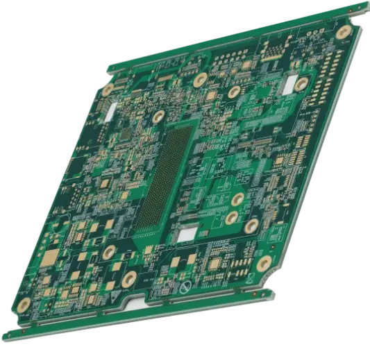
Electronic warfare has evolved from simple noise jamming to sophisticated, adaptive signal manipulation. In this high-stakes environment, the hardware must be as resilient as the software. The ECCM PCB (Electronic Counter-Countermeasures Printed Circuit Board) is the physical foundation of systems designed to resist interference and maintain communication integrity under attack.
For engineers and procurement teams, manufacturing these boards requires more than standard FR4 processes. It demands strict adherence to signal integrity, thermal management, and material stability. APTPCB (APTPCB PCB Factory) specializes in these high-reliability interconnects, ensuring that design intent translates perfectly to the battlefield.
Key Takeaways
- Definition: ECCM PCBs are specialized circuit boards designed to filter noise, resist jamming, and maintain signal fidelity in hostile electromagnetic environments.
- Material Criticality: Standard FR4 is rarely sufficient; low-loss materials (PTFE, Ceramic) are essential for preserving signal phase and amplitude.
- Signal Integrity: Controlled impedance and tight tolerance on trace width are non-negotiable to prevent signal reflection.
- Thermal Management: High-power anti-jamming transmission requires advanced heat dissipation techniques like metal cores or coin insertion.
- Validation: Testing goes beyond electrical connectivity to include TDR (Time Domain Reflectometry) and environmental stress screening.
- Partnership: Success depends on early DFM engagement with a manufacturer experienced in IPC Class 3 standards.
What ECCM PCB really means (scope & boundaries)
While the key takeaways highlight the importance of materials and testing, understanding the operational scope of an ECCM PCB is the first step in successful fabrication.
ECCM refers to the techniques used to ensure the effective use of the electromagnetic spectrum despite the enemy's use of Electronic Countermeasures (ECM). Therefore, an ECCM PCB is not a specific "type" of board like a rigid or flex board, but rather a performance class of PCB. These boards are the backbone of Battle Management PCB systems and Command Control PCB units, where a dropped signal can mean mission failure.
The scope of ECCM PCB manufacturing includes:
- Frequency Agility: The board must support rapid frequency hopping without signal degradation.
- Low Noise Floor: The laminate and layout must minimize internal crosstalk so that faint incoming signals can be distinguished from jamming noise.
- Physical Durability: These boards often reside in missiles, fighter jets, or mobile ground units, requiring resistance to high G-forces and temperature extremes.
Unlike consumer electronics, where cost is the primary driver, the primary driver here is survivability.
ECCM PCB metrics that matter (how to evaluate quality)
Once the operational scope is defined, we must quantify performance using specific manufacturing and material metrics.
The following table outlines the critical parameters that APTPCB monitors during the fabrication of ECCM-grade boards.
| Metric | Why it matters | Typical Range / Factor | How to measure |
|---|---|---|---|
| Dielectric Constant (Dk) | Determines signal propagation speed. Variations cause timing errors in phased arrays. | 2.2 to 3.5 (Stable over frequency) | IPC-TM-650 2.5.5.5 |
| Dissipation Factor (Df) | Measures how much signal is lost as heat. Lower is better for weak signal detection. | < 0.002 (Low Loss) | Cavity Resonator Method |
| CTE (z-axis) | Coefficient of Thermal Expansion. High CTE leads to via failure during thermal cycling. | < 50 ppm/°C (below Tg) | TMA (Thermomechanical Analysis) |
| Impedance Tolerance | Mismatches cause reflections, reducing the effectiveness of anti-jamming filters. | ±5% or ±7% | TDR (Time Domain Reflectometry) |
| Peel Strength | Ensures traces do not lift under high thermal stress or vibration. | > 1.05 N/mm | IPC-TM-650 2.4.8 |
| Moisture Absorption | Water changes Dk/Df. High absorption ruins high-frequency performance. | < 0.02% | Immersion / Weight test |
How to choose ECCM PCB: selection guidance by scenario (trade-offs)
Metrics provide the raw data, but the specific application environment dictates which trade-offs are acceptable during the selection process.
Different defense scenarios require prioritizing different attributes. Below are common scenarios and how to choose the right PCB configuration.
1. Airborne Radar & Jamming Pods
- Priority: Weight reduction and high-frequency performance.
- Trade-off: Higher cost for specialized materials.
- Recommendation: Use High Frequency PCB materials like Rogers or Taconic. Implement a rigid-flex design to eliminate heavy cabling and connectors.
2. Naval Command Control Systems
- Priority: Corrosion resistance and long-term reliability.
- Trade-off: Slower signal speed (if conformal coating is too thick) vs. protection.
- Recommendation: Prioritize surface finishes like ENIG or ENEPIG. Use robust conformal coating or potting. Ensure the stackup handles high humidity without delamination.
3. Man-Portable Tactical Radios
- Priority: Miniaturization and battery efficiency.
- Trade-off: Manufacturing complexity vs. size.
- Recommendation: Utilize HDI PCB technology with blind and buried vias to densify the layout. This reduces the physical footprint while maintaining signal integrity for secure comms.
4. High-Power Ground Jammers
- Priority: Thermal dissipation.
- Trade-off: Board thickness and weight vs. cooling.
- Recommendation: Use Metal Core PCBs (MCPCB) or heavy copper traces. Embed copper coins directly under high-power RF amplifiers to shunt heat away immediately.
5. Missile Guidance Systems (Expendable)
- Priority: Extreme shock resistance and short-term reliability.
- Trade-off: Longevity (not needed) vs. mechanical robustness.
- Recommendation: Focus on via reliability (Class 3 plating thickness). Use materials with a high Glass Transition Temperature (Tg) to survive the intense heat of launch.
6. Satellite / Space-Based ECCM
- Priority: Low outgassing and radiation hardness.
- Trade-off: extremely limited material choices.
- Recommendation: Select materials specifically rated for space (low outgassing). Avoid standard soldermasks that may vaporize in a vacuum.
ECCM PCB implementation checkpoints (design to manufacturing)

Selecting the right approach is only step one; rigorous execution through specific checkpoints ensures the final ECCM PCB performs as simulated.
APTPCB recommends the following checkpoint list for designers moving from CAD to CAM.
1. Material Availability Check
- Recommendation: Confirm lead times for specialized RF laminates (e.g., Rogers 4000 series) before finalizing the layout.
- Risk: Designing around a material with a 20-week lead time can stall the project.
- Acceptance: Supplier confirmation email or stock check.
2. Stackup Verification
- Recommendation: Balance copper distribution to prevent warping. Ensure prepreg layers provide adequate resin fill for high-copper designs.
- Risk: Bow and twist issues during assembly; impedance mismatches.
- Acceptance: Simulation report matching manufacturer's stackup capabilities.
3. Trace Width & Spacing (Etch Compensation)
- Recommendation: Account for etch factors. RF lines are sensitive; the manufacturer must apply compensation to the Gerber files.
- Risk: Final trace width is too narrow, increasing impedance and insertion loss.
- Acceptance: CAM engineering query (EQ) approval.
4. Via Structure & Backdrilling
- Recommendation: Use backdrilling for high-speed signals (>10 Gbps) to remove stubs that act as antennas.
- Risk: Signal reflection and resonance issues.
- Acceptance: Cross-section analysis (microsection) showing stub removal.
5. Surface Finish Selection
- Recommendation: Use ENIG (Electroless Nickel Immersion Gold) or Immersion Silver for flat surfaces and good conductivity. Avoid HASL for fine-pitch or high-frequency boards.
- Risk: Uneven pads affecting BGA assembly; signal loss at skin depth frequencies.
- Acceptance: Visual inspection and thickness measurement (X-ray).
6. Shielding & Grounding
- Recommendation: Implement via stitching (fencing) around RF lines to contain electromagnetic fields.
- Risk: Crosstalk between channels, compromising ECCM capabilities.
- Acceptance: Design Rule Check (DRC) for via spacing < 1/20th of the wavelength.
7. Thermal Stress Test
- Recommendation: Perform multiple reflow simulations.
- Risk: Delamination of hybrid stackups (e.g., FR4 bonded with PTFE).
- Acceptance: IPC-TM-650 2.6.6 (Thermal Shock).
8. Final Electrical Test
- Recommendation: 100% Netlist testing plus TDR for impedance control.
- Risk: Open/short circuits or out-of-spec impedance passing through to assembly.
- Acceptance: Certificate of Conformance (CoC) with TDR logs.
ECCM PCB common mistakes (and the correct approach)
Even with a solid plan and checklist, specific pitfalls often derail ECCM PCB projects during the NPI (New Product Introduction) phase.
1. Ignoring Hybrid Stackup CTE Mismatch
- Mistake: Mixing FR4 and PTFE materials without considering their different expansion rates (CTE).
- Result: Delamination or plated through-hole (PTH) fractures during reflow.
- Correction: Use "spread glass" or specialized bonding sheets recommended by Aerospace Defense PCB experts to buffer the stress.
2. Over-specifying Tolerances
- Mistake: Requesting ±1% impedance tolerance when ±5% is sufficient and manufacturable.
- Result: Skyrocketing costs and low yield.
- Correction: Consult with the manufacturer on standard capabilities (typically ±5% to ±10%) and design the circuit to handle slight variances.
3. Neglecting the "Skin Effect"
- Mistake: Using standard copper roughness for very high-frequency lines.
- Result: Increased insertion loss because the signal travels along the rough surface of the copper.
- Correction: Specify "Low Profile" or "Very Low Profile" (VLP) copper foil for RF layers.
4. Poor Thermal Pathing for Shields
- Mistake: Placing metal RF shields without adequate ground vias underneath.
- Result: The shield heats up and radiates energy rather than grounding it.
- Correction: Design a robust ground ring with dense via stitching where the shield will be soldered.
5. Relying on Datasheet Dk Values Only
- Mistake: Using the "Design Dk" from a datasheet without considering frequency.
- Result: The actual Dk at 10GHz is different from the Dk at 1MHz, causing phase shifts.
- Correction: Request Dk values specifically for your operating frequency from the laminate supplier (e.g., Rogers PCB materials).
6. Inadequate Fiducials for Assembly
- Mistake: Omitting fiducials on high-density boards.
- Result: Pick-and-place machines cannot align fine-pitch components accurately.
- Correction: Include global and local fiducials, especially near BGA and QFN components.
ECCM PCB FAQ (cost, lead time, Design for Manufacturability (DFM) files, stackup, impedance, Dielectric Constant (DK)/Dissipation Factor (DF))
Q: What is the difference between standard PCB and ECCM PCB? A: ECCM PCBs prioritize signal integrity, low loss, and anti-jamming capabilities using advanced materials (PTFE/Ceramic) and tighter manufacturing tolerances, whereas standard PCBs focus on connectivity and cost.
Q: Can I use FR4 for ECCM applications? A: Generally, no. Standard FR4 has a high Dissipation Factor (Df) which causes signal loss at high frequencies. However, high-performance FR4 (High-Tg, Low-Loss) might be used for non-RF layers in a hybrid stackup.
Q: What surface finish is best for high-frequency ECCM boards? A: Immersion Silver or ENIG are preferred. Immersion Silver offers the best conductivity for high-frequency signals (reducing skin effect losses), while ENIG offers excellent flatness and oxidation resistance.
Q: How does APTPCB handle hybrid stackups? A: We use specialized lamination cycles that accommodate the different curing temperatures and pressures required for dissimilar materials (e.g., bonding Teflon with FR4).
Q: What is the typical lead time for an ECCM PCB? A: It depends on material availability. If stock laminates are used, 5-10 days. If specialized Rogers or Taconic materials must be ordered, it can take 3-4 weeks.
Q: Do you support IPC Class 3 standards? A: Yes, most defense and aerospace applications, including Battle Management PCBs, require IPC Class 3, which mandates stricter criteria for plating thickness, annular rings, and visual defects.
Q: What data is needed for a controlled impedance quote? A: We need the target impedance (e.g., 50Ω), the specific layers involved, the trace width/spacing constraints, and the preferred material set.
Q: How do you test for signal integrity? A: We use TDR (Time Domain Reflectometry) coupons included on the production panel to measure the actual impedance of the traces and ensure they meet the design specifications.
ECCM PCB glossary (key terms)
| Term | Definition |
|---|---|
| ECCM | Electronic Counter-Countermeasures. Techniques to ensure effective use of the electromagnetic spectrum despite enemy jamming. |
| ECM | Electronic Countermeasures. Actions taken to prevent or reduce an enemy's effective use of the electromagnetic spectrum (jamming). |
| Dk (Dielectric Constant) | A measure of a material's ability to store electrical energy in an electric field. Affects signal speed. |
| Df (Dissipation Factor) | A measure of the power loss rate of an electrical mode in a dissipative system. Lower is better for RF. |
| Hybrid Stackup | A PCB layer buildup that uses two or more different types of laminate materials (e.g., FR4 + Rogers). |
| Backdrilling | The process of drilling out the unused portion of a plated through-hole (stub) to reduce signal reflection. |
| Skin Effect | The tendency of high-frequency alternating current to distribute itself near the surface of the conductor. |
| CTE (Coefficient of Thermal Expansion) | How much a material expands when heated. Mismatches cause reliability issues. |
| TDR (Time Domain Reflectometry) | A measurement technique used to determine the impedance of a PCB trace. |
| IPC Class 3 | The highest performance class for PCB manufacturing, intended for high-reliability products where downtime is not acceptable. |
| Vias (Blind/Buried) | Blind vias connect an outer layer to an inner layer; buried vias connect inner layers only. Used in HDI. |
| Fiducial | A copper marker on the PCB used by assembly machines for optical alignment. |
Conclusion (next steps)
Manufacturing an ECCM PCB is a discipline that merges material science with precision engineering. Whether the application is a Battle Management PCB for a naval vessel or a Command Control PCB for a mobile ground unit, the goal remains the same: absolute signal resilience in a chaotic environment.
To ensure your project moves smoothly from concept to the field, early validation is key. When you are ready to proceed, prepare your Gerber files, stackup requirements, and IPC class specifications.
Ready to manufacture? Contact APTPCB for a comprehensive DFM review. We will analyze your design for material compatibility, impedance control, and manufacturability to ensure your defense electronics perform exactly as required.