High-performance computing demands faster data transfer rates between heterogeneous chips, making EMIB interconnect board impedance control a critical factor in modern semiconductor packaging. As designs move toward 2.5D packaging and chiplet architectures, the traditional boundaries between the PCB and the package substrate blur. Ensuring signal integrity across the embedded bridge and the surrounding organic substrate requires precise manufacturing execution. This guide provides a comprehensive workflow for engineers and procurement teams to manage impedance in these advanced interconnects.
Key Takeaways
- Definition: EMIB interconnect board impedance control refers to maintaining a specific characteristic impedance (usually 85Ω or 100Ω differential) across the transition from the silicon bridge to the organic substrate.
- Critical Metric: Return loss and insertion loss are just as important as the target impedance value ($Z_0$) in high-speed chiplet integration.
- Material Impact: The mismatch in dielectric constant ($D_k$) between the silicon bridge and the PCB build-up layers is the primary source of signal reflection.
- Misconception: Many assume standard PCB tolerances (+/- 10%) are sufficient; however, EMIB designs often require +/- 5% or tighter control.
- Validation: Time Domain Reflectometry (TDR) testing must be performed on specific test coupons that mimic the bridge-to-board transition, not just standard trace coupons.
- Manufacturing Tip: Controlling copper surface roughness is essential to minimize skin effect losses at frequencies above 25 GHz.
- APTPCB (APTPCB PCB Factory) specializes in the high-precision HDI and substrate-like PCB processes required to support these advanced packaging architectures.
What EMIB interconnect board impedance control really means
Understanding the core definition is the first step before analyzing specific metrics and manufacturing tolerances.
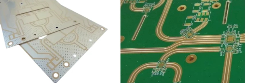
EMIB interconnect board impedance control is the engineering discipline of managing the electrical resistance to AC signals as they travel between the embedded silicon bridge and the organic package substrate. Unlike standard PCBs where traces run on uniform fiberglass layers, an EMIB (Embedded Multi-die Interconnect Bridge) structure involves a hybrid environment. Signals must traverse from a silicon die, through micro-bumps, into a silicon bridge, and out to the package substrate.
The "interconnect board" in this context acts as the carrier. It must match the impedance of the ultra-fine pitch routing on the silicon bridge. If the impedance mismatches at the interface, signal reflections occur. These reflections cause data corruption, increased bit error rates (BER), and reduced power efficiency. For APTPCB, achieving this control means utilizing advanced HDI (High Density Interconnect) techniques, laser microvias, and ultra-thin dielectric materials that bridge the gap between semiconductor manufacturing and traditional PCB fabrication.
EMIB interconnect board impedance control metrics that matter
Once the scope of impedance control is defined, engineers must quantify quality using specific performance indicators.
The success of an EMIB interconnect board design relies on strict adherence to signal integrity metrics. In high-speed applications like AI accelerators or data center processors, a simple "pass/fail" on resistance is insufficient. You must evaluate how the board behaves across a frequency spectrum.
| Metric | Why it matters | Typical Range / Factors | How to measure |
|---|---|---|---|
| Characteristic Impedance ($Z_0$) | Determines if the signal path matches the source and load. Mismatches cause reflections. | 85Ω or 100Ω (Differential); 50Ω (Single-ended). Tolerance: ±5% to ±10%. | Time Domain Reflectometry (TDR) on test coupons. |
| Insertion Loss | Measures how much signal power is lost as it travels through the interconnect. | < -1.5 dB per inch at Nyquist frequency. Heavily influenced by copper roughness and $D_k$. | Vector Network Analyzer (VNA) or S-parameter extraction. |
| Return Loss | Measures the amount of signal reflected back to the source due to impedance discontinuities. | < -10 dB to -15 dB is desirable. Lower is better. | VNA (S11 parameter). |
| Skew (Intra-pair) | The time delay difference between the positive and negative lines of a differential pair. | < 5 ps (picoseconds). Critical for differential signaling. | TDR or Oscilloscope. |
| Dielectric Constant ($D_k$) Stability | Variations in $D_k$ cause impedance fluctuations along the trace. | Stable $D_k$ across frequency (e.g., 3.0 - 3.5 for advanced substrates). | Material datasheet verification and resonator rings. |
| Copper Surface Roughness | Rough copper increases resistance at high frequencies (Skin Effect). | $R_z$ < 2 µm (VLP or HVLP copper foil recommended). | Profilometer or SEM (Scanning Electron Microscope). |
How to choose EMIB interconnect board impedance control: selection guidance by scenario
With the metrics established, the next challenge is selecting the right control strategy based on the specific application scenario.
Different end-use cases require different levels of rigor in EMIB interconnect board impedance control. Over-specifying adds unnecessary cost, while under-specifying leads to system failure.
Scenario 1: High-Performance Computing (HPC) & AI
- Requirement: Maximum bandwidth (HBM integration).
- Trade-off: Requires the tightest impedance tolerance (±5%) and ultra-low loss materials.
- Guidance: Choose advanced build-up films (ABF) and HVLP copper. Cost is secondary to performance.
Scenario 2: Consumer Mobile Devices
- Requirement: Miniaturization and battery life.
- Trade-off: Space constraints force thinner dielectrics, making impedance harder to control.
- Guidance: Prioritize thin core materials. Accept slightly looser tolerances (±7-10%) to maintain yield and lower cost.
Scenario 3: Automotive ADAS Systems
- Requirement: Reliability and thermal stability.
- Trade-off: Materials must withstand thermal cycling, which can shift impedance over time.
- Guidance: Select high-Tg materials with stable $D_k$ over wide temperature ranges. Validation must include thermal stress testing.
Scenario 4: 5G Infrastructure / Base Stations
- Requirement: High frequency and low latency.
- Trade-off: Long trace lengths on the substrate increase insertion loss risks.
- Guidance: Focus on "Low Loss" and "Ultra Low Loss" laminates. Impedance control must account for the specific frequency bands (mmWave).
Scenario 5: Prototype / NPI (New Product Introduction)
- Requirement: Speed of delivery and debugging.
- Trade-off: Quick turns might limit material availability.
- Guidance: Use standard available high-speed materials. Focus on validating the design logic rather than perfect impedance optimization.
Scenario 6: Mass Production (Cost Sensitive)
- Requirement: Yield and cost efficiency.
- Trade-off: Cannot sustain ultra-tight tolerances without high scrap rates.
- Guidance: Design for Manufacturing (DFM). Widen traces where possible to make impedance less sensitive to etching variations.
EMIB interconnect board impedance control implementation checkpoints
After selecting the right strategy, the focus shifts to the tactical execution from design files to the final product.
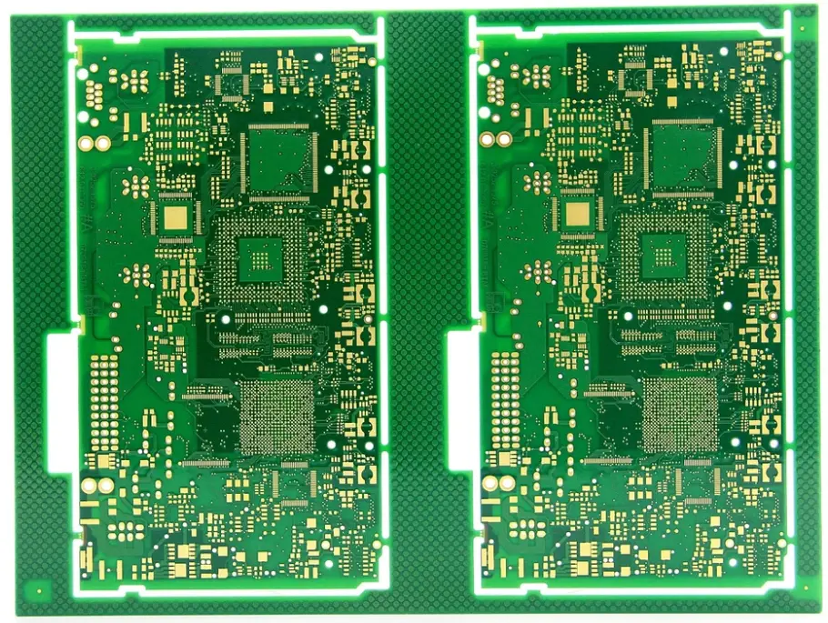
Implementing EMIB interconnect board impedance control requires a synchronized effort between the layout engineer and the manufacturing floor. Use this checklist to ensure no critical step is missed during the HDI PCB fabrication process.
Stackup Definition:
- Recommendation: Define layer counts, dielectric thicknesses, and copper weights explicitly.
- Risk: Ambiguous stackups lead to incorrect impedance calculations by the CAM engineer.
- Acceptance: Approved stackup sheet signed by both designer and fab.
Material Selection:
- Recommendation: Specify exact material series (e.g., Megtron 6, Rogers, or specific ABF films).
- Risk: Generic "FR4" callouts will fail at EMIB speeds.
- Acceptance: Material certification (CoC) from the supplier.
Trace Width and Spacing (L/S):
- Recommendation: Adjust trace width in CAM to compensate for etch factors (trapezoidal shape).
- Risk: Over-etching reduces trace width, raising impedance.
- Acceptance: Cross-section analysis (micro-section) verifying geometry.
Reference Plane Continuity:
- Recommendation: Ensure solid ground planes beneath high-speed signals, especially near the bridge interface.
- Risk: Splits in the reference plane cause immediate impedance discontinuities.
- Acceptance: Automated Optical Inspection (AOI) of inner layers.
Microvia Registration:
- Recommendation: Laser drilling alignment must be precise to connect the bridge pads to the substrate.
- Risk: Misalignment changes the capacitive coupling, altering impedance.
- Acceptance: X-ray inspection of via alignment.
Copper Plating Thickness:
- Recommendation: Maintain uniform plating distribution.
- Risk: Variations in copper thickness affect the total inductance of the line.
- Acceptance: Non-destructive thickness measurement (CMI).
Surface Finish Application:
- Recommendation: Use ENIG or ENEPIG for flat surfaces suitable for wire bonding or flip-chip.
- Risk: Thick HASL finishes create uneven surfaces and impedance variations.
- Acceptance: Surface finish thickness measurement (XRF).
Etch Compensation:
- Recommendation: The factory must apply global etch compensation based on copper weight.
- Risk: Inconsistent etching across the panel leads to impedance variation between units.
- Acceptance: Impedance coupon testing on panel edges.
Solder Mask Effect:
- Recommendation: Account for the $D_k$ of the solder mask in the impedance calculation (for outer layers).
- Risk: Solder mask reduces impedance by 2-3 ohms; ignoring this causes failures.
- Acceptance: TDR measurement after solder mask application.
Final TDR Validation:
- Recommendation: 100% testing of impedance coupons for critical batches.
- Risk: Shipping boards that pass electrical continuity but fail signal integrity.
- Acceptance: TDR report showing pass/fail against tolerance.
EMIB interconnect board impedance control common mistakes
Even with a checklist, specific errors frequently occur in the complex environment of embedded bridge manufacturing.
Avoiding these common pitfalls in EMIB interconnect board impedance control can save weeks of redesign time and thousands of dollars in scrap.
- Ignoring the "Transition Zone": The most critical impedance discontinuity happens where the signal moves from the silicon bridge to the PCB substrate. Designers often match the trace impedance but ignore the parasitic capacitance of the landing pad/bump. Correction: Simulate the transition in 3D field solvers and optimize the pad stack.
- Using Generic Dielectric Constants: Relying on the "marketing" $D_k$ value (e.g., 4.0) instead of the frequency-dependent value (e.g., 3.8 at 10 GHz). Correction: Request the frequency-dependent material table from APTPCB.
- Neglecting Copper Roughness Models: Standard impedance calculators assume smooth copper. At EMIB speeds, roughness adds significant delay and loss. Correction: Use the Huray model or similar roughness correction factors in calculations.
- Inadequate Test Coupons: Placing test coupons too far from the actual circuitry or using designs that don't match the actual trace density. Correction: Use embedded coupons or "in-circuit" testing structures where possible.
- Overlooking Manufacturing Tolerances: Designing a 50-ohm line that requires a 3.1 mil trace, when the factory's minimum capability is 3 mil +/- 0.5 mil. Correction: Consult the Impedance Calculator and design rules early.
- Failing to Account for Resin Rich areas: In heterogeneous substrates, resin can pool in gaps between traces, changing the local $D_k$. Correction: Use dummy copper fill (thieving) to ensure uniform resin distribution and pressing.
EMIB interconnect board impedance control FAQ
To wrap up the technical details, here are answers to the most pressing questions regarding logistics and execution.
Q: How does strict EMIB interconnect board impedance control impact the overall cost? A: Tightening tolerances from ±10% to ±5% can increase costs by 15-25%. This is due to the need for higher-grade materials, more frequent TDR testing, and lower manufacturing yields.
Q: What is the typical lead time for EMIB interconnect board prototypes with impedance requirements? A: Standard lead times are 15-20 days. However, if specialized low-loss materials or ABF films are required, lead times can extend to 4-6 weeks depending on material availability.
Q: Which materials are best for EMIB interconnect board impedance control at 56Gbps? A: Standard FR4 is not suitable. You should use materials like Panasonic Megtron 6/7, Isola Tachyon, or specialized Ajinomoto Build-up Films (ABF) that offer low Loss Tangent ($D_f$) and stable $D_k$.
Q: How is testing performed for buried layers in an EMIB substrate? A: Testing buried layers is difficult on the finished board. We use "test coupons" located on the panel rails that have the same layer structure and trace geometry as the actual board. These are tested via TDR before the outer layers are laminated or after final fabrication.
Q: What are the acceptance criteria for TDR testing on these boards? A: The standard acceptance criterion is that the measured impedance must fall within the specified tolerance (e.g., 100Ω ±10%). Additionally, the TDR waveform should be smooth, without sharp dips or spikes indicating discontinuities.
Q: Can I use standard vias for EMIB interconnect board design? A: Generally, no. EMIB designs require high-density routing that necessitates laser microvias, blind vias, and buried vias to manage signal integrity and density. Mechanical drills are often too large and create too much parasitic capacitance.
Q: How do I specify impedance control in my Gerber files? A: Do not rely on Gerber filenames alone. Include a detailed fabrication drawing (Fab Drawing) that lists the specific layers, trace widths, reference planes, and target impedance values for each signal group.
Q: What is the difference between single-ended and differential impedance in this context? A: Single-ended impedance references a trace to a ground plane (usually 50Ω). Differential impedance references two traces to each other and the ground plane (usually 85Ω or 100Ω). EMIB data paths are almost exclusively differential to reject noise.
Resources for EMIB interconnect board impedance control
- High Speed PCB Manufacturing: Explore capabilities for manufacturing boards that support high data rates.
- Impedance Calculator: A tool to estimate trace width and spacing for your target impedance.
- HDI PCB Technology: Learn about the microvia and fine-line technologies essential for EMIB substrates.
- PCB Stackup Design: Guidelines on arranging layers to achieve optimal signal integrity.
EMIB interconnect board impedance control glossary
| Term | Definition |
|---|---|
| EMIB | Embedded Multi-die Interconnect Bridge. A technology using a silicon bridge embedded in a substrate to connect dies. |
| Impedance ($Z_0$) | The opposition a circuit presents to the passage of a current when a voltage is applied. |
| TDR | Time Domain Reflectometry. A measurement technique used to determine the impedance of a line. |
| Microvia | A small hole drilled by a laser (typically < 150µm) to connect adjacent layers in HDI boards. |
| ABF | Ajinomoto Build-up Film. A dominant insulation material used in IC substrates for high-performance CPUs/GPUs. |
| CTE | Coefficient of Thermal Expansion. The rate at which a material expands with heat. Mismatches cause reliability issues. |
| Insertion Loss | The loss of signal power resulting from the insertion of a device (or trace) in a transmission line. |
| Return Loss | The loss of power in the signal returned/reflected by a discontinuity in a transmission line. |
| Differential Pair | Two complementary signals used to transmit data, offering high noise immunity. |
| Skin Effect | The tendency of high-frequency alternating current to distribute itself near the surface of the conductor. |
| Dielectric Constant ($D_k$) | A measure of a material's ability to store electrical energy in an electric field. Affects signal speed and impedance. |
| Loss Tangent ($D_f$) | A measure of signal power lost as heat within the dielectric material. |
| RDL | Redistribution Layer. Metal layers on a die or substrate that reroute I/O pads to different locations. |
Conclusion (next steps)
Mastering EMIB interconnect board impedance control is a prerequisite for competing in the era of chiplets and heterogeneous integration. It requires a shift in mindset from "connecting points" to "managing transmission lines." By understanding the metrics of insertion loss and return loss, selecting the right materials, and enforcing strict manufacturing checkpoints, you can ensure your high-performance designs function as intended.
If you are ready to move your design from concept to production, APTPCB is ready to assist. To get an accurate DFM review and quote, please provide the following:
- Gerber Files (RS-274X) or ODB++ data.
- Stackup Diagram indicating desired materials and layer count.
- Impedance Requirements (e.g., Layer 3, 100Ω Diff, Trace width 4mil).
- Netlist for electrical testing validation.
Visit our Quote Page to start your project today.