Definition, scope, and who this guide is for
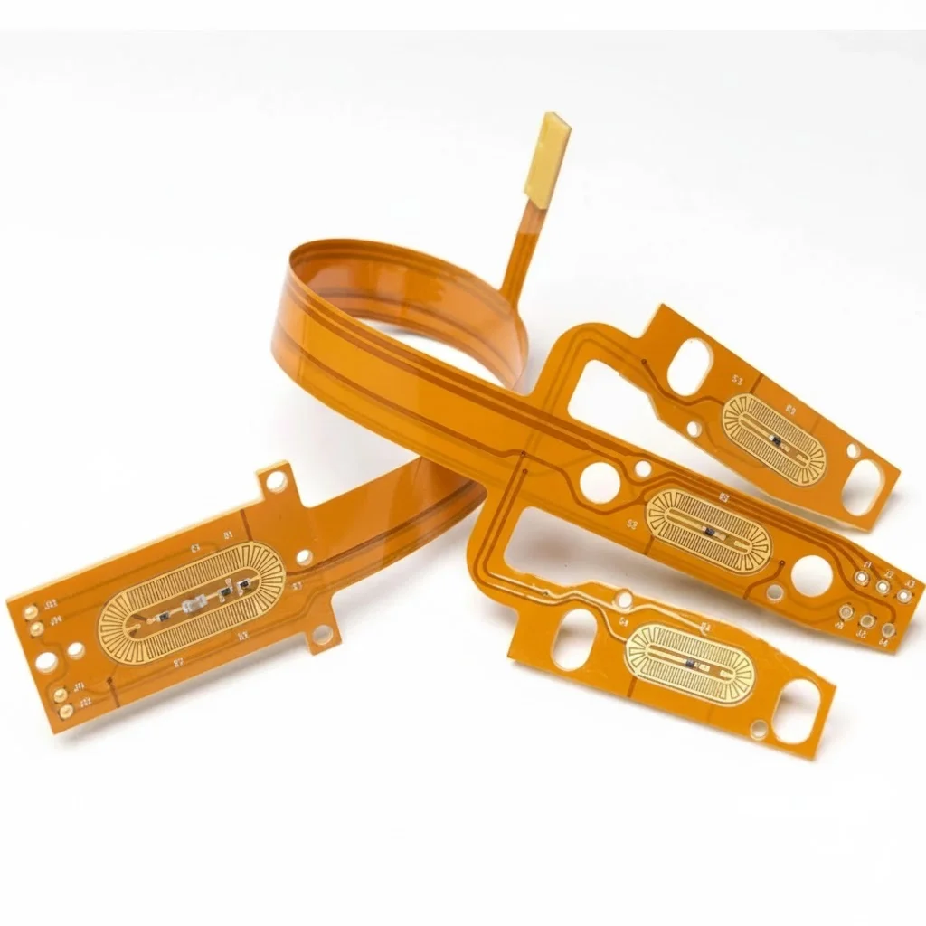
EtherCAT interface PCB design refers to the specialized engineering and layout processes required to implement the EtherCAT (Ethernet for Control Automation Technology) protocol on a printed circuit board. Unlike standard office Ethernet, EtherCAT operates in harsh industrial environments requiring real-time data transmission with microsecond-level synchronization. The scope of this design work encompasses the physical layer (PHY) layout, differential pair routing, impedance control, magnetic isolation, and robust grounding strategies to prevent packet loss in electrically noisy settings.
This playbook is written for hardware engineers, technical procurement leads, and product managers who are transitioning a prototype into mass production. It moves beyond basic schematic theory to focus on manufacturability, reliability, and supply chain validation. You will find actionable specifications to include in your documentation, a breakdown of common failure modes during scale-up, and a rigorous checklist to ensure your manufacturing partner can deliver consistent quality.
At APTPCB (APTPCB PCB Factory), we often see designs fail not because of logic errors, but because of physical layout issues that compromise signal integrity under stress. This guide aims to bridge the gap between a functional datasheet and a robust, field-ready product. By following these steps, you reduce the risk of communication dropouts (CRC errors) and ensure your industrial automation equipment meets the stringent reliability standards expected in the market.
When to use EtherCAT interface PCB design (and when a standard approach is better)
Understanding the specific demands of industrial protocols is the first step before diving into the technical specifications of your board.
While standard Ethernet layout guidelines provide a baseline, EtherCAT interface PCB design is mandatory when your application involves motion control, robotics, or real-time I/O where latency must be deterministic. Standard Ethernet (TCP/IP) can tolerate re-sent packets and variable latency; EtherCAT cannot. If a packet is lost or delayed due to poor signal integrity, the entire control loop may fault, causing machine downtime. Therefore, if your device acts as an EtherCAT Slave or Master in a factory automation environment, you must adopt the strict impedance and shielding practices outlined here.
Conversely, a standard, less rigorous Ethernet design approach might suffice for administrative data ports or non-real-time logging interfaces where the environment is controlled (e.g., a server room) and occasional latency is acceptable. However, for the actual EtherCAT ports (IN/OUT), the "standard" approach is often a recipe for intermittent field failures. The cost of a specialized design is negligible compared to the cost of debugging intermittent sync loss in a deployed industrial machine.
EtherCAT interface PCB design specifications (materials, stackup, tolerances)
Once you have determined that a robust EtherCAT implementation is necessary, the next step is to translate performance needs into concrete manufacturing specifications.
Defining these requirements early prevents "engineering by assumption" where the fabricator guesses your needs. Include these 8–12 specifications in your fabrication drawing and RFQ to ensure the EtherCAT interface PCB design is executed correctly:
- Differential Impedance Control: Specify 100Ω ±10% for all differential pairs (TX+/TX-, RX+/RX-). This is the single most critical factor for signal integrity.
- Single-Ended Impedance: Define 50Ω ±10% for MII/RMII/RGMII clock and data lines connecting the EtherCAT Slave Controller (ESC) to the PHY.
- PCB Stackup Strategy: Mandate a minimum 4-layer board for any EtherCAT design. Layers 2 and 3 should serve as solid Ground and Power planes to provide a return path for high-speed signals.
- Copper Weight: Standard 1 oz (35µm) is usually sufficient for signal layers, but ensure power planes can handle the current if the board also drives motors or heavy I/O.
- Material Selection: Use FR-4 High Tg (Tg > 170°C) if the device operates in industrial cabinets with high ambient temperatures. Standard Tg (130-140°C) may cause barrel cracking under thermal cycling.
- Trace Width and Spacing: Explicitly state the trace width and spacing required to achieve the target impedance based on the supplier's stackup. Typically, this is around 4-6 mil width / 5-8 mil spacing.
- Pair Length Matching (Skew): Require intra-pair skew to be less than 5 mils (0.127mm) to prevent phase shifts that close the data eye.
- Inter-Pair Length Matching: Keep transmit and receive pairs matched within 2 inches (50mm), though this is less critical than intra-pair skew.
- Isolation Voltage: Specify a clearance on the PCB layout to support 1.5 kVrms isolation between the chassis ground (shield) and the digital ground, typically achieved via the magnetics and a physical void in the PCB planes.
- Via Types: Specify standard through-hole vias. Avoid blind/buried vias unless density absolutely demands it, as they increase cost and complexity without benefiting signal integrity at 100Mbps.
- Surface Finish: Choose ENIG (Electroless Nickel Immersion Gold) for flat pads, which helps with the precise soldering of fine-pitch PHY chips and RJ45 connectors.
- Solder Mask Color: While often aesthetic, avoid black or white matte masks for initial prototypes as they make visual inspection of traces difficult; Green or Blue is preferred for NPI.
EtherCAT interface PCB design manufacturing risks (root causes and prevention)
With specifications defined, you must now anticipate where the design might fail when moving from 5 prototypes to 5,000 units.
Scale-up risks in EtherCAT interface PCB design often stem from process variations and environmental stressors that didn't appear on the lab bench.
- Impedance Mismatch due to Etching Variation:
- Why it happens: During mass production, over-etching can narrow traces, raising impedance above 110Ω.
- Detection: Signal reflections, increased Bit Error Rate (BER).
- Prevention: Require TDR (Time Domain Reflectometry) coupons on every production panel and request a TDR report.
- Crystal Oscillator Startup Failure:
- Why it happens: Stray capacitance from flux residue or poor layout prevents the PHY clock from starting reliably.
- Detection: Device fails to link up periodically or is dead on arrival.
- Prevention: Keep crystal traces ultra-short (<10mm), surround with ground guard rings, and ensure the PCB assembly process includes thorough washing (if not using no-clean flux).
- ESD Damage to PHY:
- Why it happens: Industrial environments have high static. If the TVS diodes are placed too far from the connector, the spike hits the PHY first.
- Detection: Permanent port failure after handling or installation.
- Prevention: Place ESD protection devices immediately next to the connector pins. Route signals through the protection pads, not just "tee" them off.
- Magnetics Saturation or Failure:
- Why it happens: Using low-quality discrete magnetics or integrated RJ45s that cannot handle DC bias or temperature extremes.
- Detection: Packet loss increases significantly at high temperatures.
- Prevention: Validate magnetics against the PHY manufacturer’s recommended list. Do not swap magnetics for a "cheaper equivalent" without testing.
- Ground Loops / Shielding Issues:
- Why it happens: Incorrect coupling between Chassis Ground and Digital Ground (e.g., missing the 1MΩ resistor + capacitor parallel circuit).
- Detection: Communication drops when nearby motors or VFDs start up.
- Prevention: Strictly follow the "Bob Smith Termination" and isolation guidelines. Ensure the RJ45 shield is connected to Chassis Ground, not Digital Ground directly.
- Connector Mechanical Fatigue:
- Why it happens: RJ45 connectors rely on solder joints for mechanical strength. Heavy cables vibrate in industrial settings, cracking joints.
- Detection: Intermittent connection when the cable is wiggled.
- Prevention: Use connectors with through-hole shield tabs for mechanical anchoring, even if the signal pins are SMT.
- Thermal Throttling of PHY:
- Why it happens: Modern PHYs run hot. If the PCB lacks thermal vias under the exposed pad (QFN packages), heat accumulates.
- Detection: Link drops after 30-60 minutes of operation.
- Prevention: Place a dense array of thermal vias connected to the ground plane directly under the PHY component.
- Reference Plane Discontinuities:
- Why it happens: Routing differential pairs over a split in the ground plane (e.g., crossing from 3.3V to 5V plane areas).
- Detection: High EMI emissions and poor signal integrity.
- Prevention: Ensure differential pairs run over a solid, unbroken ground reference plane for their entire length.
- Skew from Fiber Weave Effect:
- Why it happens: On very high-speed lines (Gigabit EtherCAT G), the glass weave pattern in FR4 can cause one leg of the pair to travel faster than the other.
- Detection: Jitter and eye-diagram closure.
- Prevention: For standard 100Mbps EtherCAT, this is rare. For Gigabit, route traces at a slight angle (zigzag) relative to the weave.
- Flux Residue under BGA/QFN:
- Why it happens: Poor cleaning under low-clearance components causes leakage currents.
- Detection: Unstable operation in humid environments.
- Prevention: Use reputable assembly houses with verified wash processes or qualified no-clean pastes.
EtherCAT interface PCB design validation and acceptance (tests and pass criteria)

Preventing risks requires a structured validation plan that confirms the EtherCAT interface PCB design meets all physical and functional requirements.
This plan should be executed during the NPI (New Product Introduction) phase before signing off on mass production.
- TDR Impedance Verification:
- Objective: Confirm trace manufacturing accuracy.
- Method: Measure test coupons provided by the fab house.
- Criteria: 100Ω ±10% for differential pairs; 50Ω ±10% for single-ended.
- DC Resistance & Continuity Test:
- Objective: Ensure no opens/shorts in the signal path.
- Method: Automated flying probe or bed-of-nails test.
- Criteria: 100% pass on all nets.
- Signal Integrity (Eye Diagram) Test:
- Objective: Validate the quality of the physical signal.
- Method: Use an oscilloscope with a differential probe at the PHY TX pins.
- Criteria: The "eye" must be wide open, meeting the IEEE 802.3 mask requirements. No overshoot >10%.
- Packet Error Rate Test (BERT):
- Objective: Test functional reliability over time.
- Method: Run an EtherCAT master loop sending millions of packets for 24-48 hours.
- Criteria: Zero lost packets (CRC errors) over the duration.
- Thermal Stress Test:
- Objective: Verify stability under heat.
- Method: Operate the device in a chamber at max rated temp (e.g., 85°C) for 4 hours.
- Criteria: No link drops; PHY temperature remains within datasheet limits.
- Vibration/Shock Test:
- Objective: Validate connector mechanical robustness.
- Method: Random vibration profile (e.g., 5-500Hz) while the link is active.
- Criteria: No physical cracking; no momentary link loss.
- EMC/EMI Pre-compliance Scan:
- Objective: Ensure the device doesn't radiate excessive noise.
- Method: Near-field probe scan over the connector and PHY area.
- Criteria: Emissions should be 3-6dB below the Class A/B limit lines.
- ESD Immunity Test:
- Objective: Verify protection diodes.
- Method: Apply contact discharge (±4kV) and air discharge (±8kV) to the connector shield and pins.
- Criteria: Device may reset but must self-recover; no permanent damage.
- Isolation (Hi-Pot) Test:
- Objective: Verify galvanic isolation.
- Method: Apply 1500V AC between the Ethernet cable side and the circuit side.
- Criteria: Leakage current < 1mA; no breakdown.
- Interoperability Check:
- Objective: Ensure compatibility with different masters.
- Method: Connect to TwinCAT (Beckhoff), Omron, and other standard masters.
- Criteria: Successful enumeration and Operational (OP) state transition.
EtherCAT interface PCB design supplier qualification checklist (RFQ, audit, traceability)
To execute the validation plan successfully, you need a manufacturing partner capable of adhering to your strict EtherCAT interface PCB design requirements.
Use this checklist to vet potential suppliers. If they cannot answer these questions confidently, they are likely not a fit for industrial communication electronics.
Group 1: RFQ inputs for EtherCAT interface PCB design (What you send)
- Gerber Files: RS-274X format, clear and error-free.
- Fabrication Drawing: Clearly stating IPC Class 2 or 3 requirements.
- Stackup Definition: Explicit layer order, material type, and thickness.
- Impedance Table: Listing layer, trace width, spacing, and target impedance.
- Drill Chart: Defining finished hole sizes and tolerances.
- Pick & Place File: Centroid data for assembly.
- BOM (Bill of Materials): With approved vendor list (AVL) for critical parts like PHYs and Magnetics.
- Test Requirements: Specific instructions for TDR and functional testing.
Group 2: Capability evidence for EtherCAT interface PCB design (What they must demonstrate)
- Impedance Control: Can they achieve ±10% tolerance? Do they have in-house TDR equipment?
- Minimum Trace/Space: Can they reliably etch 4mil/4mil if required for high-density PHYs?
- Material Stock: Do they stock High-Tg FR4 and materials suitable for industrial temps?
- Small Pitch Assembly: Can they handle 0.5mm pitch QFNs or BGAs used for EtherCAT controllers?
- X-Ray Inspection: Do they have X-Ray capability to inspect solder joints under QFN/BGA chips?
- Conformal Coating: Do they offer coating services for harsh environment protection?
Group 3: Quality System & Traceability
- Certifications: ISO 9001 is mandatory; IATF 16949 is a bonus for industrial/auto.
- IPC Standards: Do they train staff to IPC-A-600 (PCB) and IPC-A-610 (Assembly)?
- Incoming QC: How do they verify the authenticity of chips (to avoid fake PHYs)?
- Solder Paste Inspection (SPI): Is SPI used on every board to prevent solder defects?
- AOI (Automated Optical Inspection): Is AOI performed post-reflow?
- Traceability: Can they trace a specific PCB serial number to the batch of raw laminate used?
Group 4: Change Control & Delivery
- PCN (Product Change Notification): Will they notify you before changing solder mask brand or laminate supplier?
- EQ (Engineering Questions): Do they review files and ask DFM questions before starting? (Silence is a red flag).
- Lead Time: Is the lead time consistent for the volumes you expect?
- Packaging: Do they use ESD-safe, vacuum-sealed packaging with desiccant?
- Logistics: Can they ship DDP (Delivered Duty Paid) if you are international?
How to choose EtherCAT interface PCB design (trade-offs and decision rules)
In EtherCAT interface PCB design, engineering is the art of compromise. Here is how to navigate common trade-offs.
- Integrated Magnetics (MagJack) vs. Discrete Magnetics:
- If you prioritize space saving and ease of layout: Choose Integrated MagJacks. They save board space and reduce component count.
- If you prioritize thermal performance and isolation reliability: Choose Discrete Magnetics. They allow better heat dissipation and higher isolation voltage ratings, often preferred in high-vibration environments.
- 4-Layer vs. 6-Layer Stackup:
- If you prioritize cost: Choose 4-Layer. It is sufficient for most 100Mbps EtherCAT designs if routed carefully.
- If you prioritize EMI performance and density: Choose 6-Layer. The extra ground planes provide superior shielding and easier routing for complex ESCs with many GPIOs.
- M12 Connectors vs. RJ45 Connectors:
- If you prioritize IP67 (water/dust) protection: Choose M12 Connectors. They are the standard for "outside the cabinet" industrial wiring.
- If you prioritize cost and standard cabling: Choose RJ45 Connectors. They are ubiquitous and cheap but generally require an IP20 (clean cabinet) environment.
- Shielded (STP) vs. Unshielded (UTP) Design:
- If you prioritize noise immunity: Design for Shielded (STP). Ensure the connector shield is grounded correctly to the chassis.
- If you prioritize cabling cost: Design for Unshielded (UTP). However, EtherCAT strongly recommends shielded cables in industrial zones.
- Hard Gold vs. ENIG Surface Finish:
- If you prioritize connector insertion durability (edge fingers): Choose Hard Gold.
- If you prioritize solderability of SMT parts: Choose ENIG. For most EtherCAT boards, ENIG is the standard choice unless the PCB itself plugs into a backplane.
EtherCAT interface PCB design FAQ (cost, lead time, Design for Manufacturability (DFM) files, stackup, impedance, Automated Optical Inspection (AOI) inspection)
Q: Can I route EtherCAT signals on the bottom layer? A: Yes, provided you have a solid ground reference plane adjacent to the bottom layer (e.g., Layer 3 in a 4-layer board). Avoid routing high-speed signals on outer layers without a reference plane.
Q: What is the maximum trace length for EtherCAT differential pairs? A: While the standard allows for long cables (100m), PCB traces should be kept as short as possible to minimize attenuation. Ideally, keep PHY-to-Magnetics traces under 4 inches (100mm).
Q: Do I need to terminate unused pairs in the RJ45 connector? A: Yes. For 10/100 Mbps EtherCAT, the unused pairs (4,5 and 7,8) should be terminated to ground via "Bob Smith" termination resistors (75Ω) and a high-voltage capacitor to reduce EMI.
Q: How do I handle the "Earth Ground" vs "Signal Ground"? A: Signal Ground (GND) is for your chips. Earth/Chassis Ground is for the shield. Connect them near the connector using a 1MΩ resistor and a 1-2kV capacitor in parallel to bleed static but block low-frequency noise loops.
Q: Is impedance control really necessary for short traces? A: Yes. Even on short traces, impedance mismatches cause reflections. While a 1cm trace might not fail immediately, it reduces the noise margin, making the device susceptible to external industrial noise.
Q: Can I use a standard Ethernet PHY for EtherCAT? A: Generally, yes. EtherCAT uses standard IEEE 802.3 physical layers. However, ensure the PHY supports the MII/RMII interface required by your specific EtherCAT Slave Controller (ESC).
Q: What is the best way to route the differential pairs? A: Route them tightly coupled (close together), symmetrical, and avoid vias if possible. If vias are needed, place them close to the pins and ensure ground vias are placed nearby to maintain the return path.
Q: Why does my EtherCAT device fail when the motor starts? A: This is likely a grounding issue. The motor noise is coupling into your board. Check your shield termination and ensure your reset line to the PHY is not picking up noise (add a capacitor to the reset pin).
Resources for EtherCAT interface PCB design (related pages and tools)
To further assist in your design and procurement process, utilize these resources:
- Industrial Control PCB Manufacturing – Understand the broader requirements for industrial-grade boards beyond just the interface.
- Impedance Calculator – A quick tool to estimate your trace width and spacing before finalizing the stackup.
- DFM Guidelines – Comprehensive design-for-manufacturing rules to ensure your layout is buildable at scale.
- Turnkey PCB Assembly – Learn how combining PCB fab and assembly can reduce logistics risks for complex NPIs.
- High-Speed PCB Design – Deeper technical insights into signal integrity for high-frequency protocols.
Request a quote for EtherCAT interface PCB design (Design for Manufacturability (DFM) review + pricing)
Ready to move your EtherCAT interface PCB design from concept to reality? APTPCB offers a complimentary DFM review with every quote to catch impedance and layout issues before they become costly scrap.
What to send for an accurate quote:
- Gerber Files (RS-274X)
- BOM (for assembly)
- Stackup & Impedance Requirements
- Quantity & Lead Time needs
Click here to Request a Quote & DFM Review
Conclusion (next steps)
Successfully deploying an EtherCAT interface PCB design requires more than just connecting pins on a schematic; it demands a holistic approach to signal integrity, mechanical robustness, and supply chain validation. By defining strict impedance specs, anticipating scale-up risks like thermal management and ESD, and rigorously validating your supplier's capabilities, you secure the reliability of your industrial automation product. Follow the checklist provided, validate early, and choose a manufacturing partner who understands the precision required for real-time industrial communication.