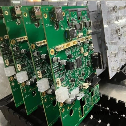
The rapid expansion of electric vehicle infrastructure has shifted the focus of electronics manufacturing toward high-power, high-reliability systems. At the heart of every charging station—whether a residential wall box or a highway supercharger—lies the EV Charger PCB. This circuit board is not merely a carrier for components; it is the critical junction managing power conversion, safety monitoring, and communication between the grid and the vehicle.
Designing and manufacturing these boards requires a departure from standard consumer electronics practices. The voltages are higher, the thermal loads are more intense, and the failure tolerance is effectively zero. Engineers must navigate complex trade-offs between copper weight, dielectric materials, and spacing rules to ensure safety and longevity.
At APTPCB (APTPCB PCB Factory), we have observed that the most successful projects prioritize Design for Manufacturing (DFM) early in the development cycle. This guide serves as a comprehensive resource for engineers and procurement teams. We will cover everything from defining the scope of an EV PCB to the specific metrics that validate its quality.
Key Takeaways
- System Complexity: An EV charger is rarely a single board; it is a system comprising power conversion, control logic, and communication modules.
- Safety First: High-voltage clearance and creepage distances are the non-negotiable foundations of EV Charger PCB design.
- Thermal Management: Heavy copper and metal core substrates are often required to handle currents ranging from 32A to over 500A.
- Material Criticality: Standard FR4 is often insufficient; materials with high CTI (Comparative Tracking Index) and high Tg (Glass Transition Temperature) are essential.
- Validation: Rigorous testing, including Hi-Pot and thermal cycling, ensures the board survives harsh outdoor environments.
- Manufacturing Partner: Working with a specialized manufacturer like APTPCB ensures adherence to automotive standards like IATF 16949.
What Electric Vehicle (EV) Charger PCB really means (scope & boundaries)
Having established the high-level importance of these components, we must first define exactly what constitutes an EV Charger PCB within the broader charging ecosystem.
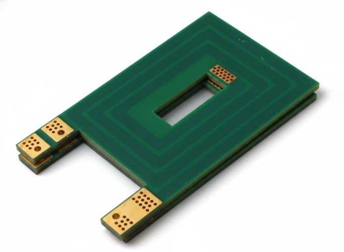
The term is often used as a catch-all, but in practice, it refers to a cluster of specialized boards working in unison. A robust charging station is not a monolith; it is a distributed system. Understanding this segmentation is vital for selecting the right materials for each sub-assembly.
The Power Conversion Board (EV Converter PCB)
This is the "muscle" of the system. In DC fast chargers, this board handles the rectification (AC to DC) and voltage regulation. It deals with high voltages (400V to 800V+) and high currents.
- Primary Function: Power switching, rectification, and filtering.
- Key Characteristic: Heavy copper traces, wide spacing, and robust thermal management.
The Control Unit (EV Controller PCB)
If the converter is the muscle, this is the brain. It manages the charging logic, safety protocols, and user interface. It monitors the state of the battery and adjusts the current flow accordingly.
- Primary Function: Logic processing, safety monitoring, and relay control.
- Key Characteristic: High-density interconnects (HDI), fine pitch components, and signal integrity focus.
The Communication Module (EV Gateway PCB)
Modern chargers are IoT devices. They communicate with the backend network for billing and with the vehicle for handshake protocols (like ISO 15118).
- Primary Function: Wi-Fi, 4G/5G, Bluetooth, and PLC (Power Line Communication).
- Key Characteristic: Impedance control and RF shielding.
The Battery Interface (EV Battery PCB)
While technically part of the vehicle's Battery Management System (BMS), the charger must interface seamlessly with this board. The charger PCB must interpret signals from the EV Battery PCB to prevent overcharging or thermal runaway.
By breaking down the "EV Charger PCB" into these specific categories, designers can apply the correct IPC standards and material choices to each section rather than over-engineering the entire system.
Electric Vehicle (EV) Charger PCB metrics that matter (how to evaluate quality)
Understanding the scope is the first step; measuring quality through specific technical metrics is the second.
In the automotive and high-power energy sectors, vague terms like "good quality" are insufficient. You need quantifiable data to predict how an EV Charger PCB will perform under load. The following metrics are the primary indicators of a board's suitability for EV applications.
| Metric | Why it matters | Typical Range / Factor | How to Measure |
|---|---|---|---|
| CTI (Comparative Tracking Index) | Determines the PCB's resistance to electrical breakdown (tracking) across the surface under voltage. Crucial for safety in high-voltage chargers. | PLC 0 (600V+) is standard for EV chargers. Standard FR4 is often only 175V. | IEC 60112 standard test method. |
| Tg (Glass Transition Temperature) | The temperature at which the PCB material turns from hard to soft. High heat from charging requires high Tg to prevent delamination. | >170°C (High Tg) is recommended. Standard is 130-140°C. | DSC (Differential Scanning Calorimetry) or TMA. |
| Copper Weight | Defines the current-carrying capacity. Thicker copper reduces resistance and heat generation. | 2 oz to 6 oz (or more). Standard electronics use 1 oz. | Micro-section analysis or weight measurement. |
| Dielectric Breakdown Voltage | The maximum voltage the insulation can withstand before conducting. Essential for layer-to-layer isolation. | >1000V/mil. Total stackup must exceed system peak voltage + safety margin. | Hi-Pot testing (High Potential). |
| Thermal Conductivity | How efficiently the material transfers heat away from components. Critical for Metal Core PCBs (MCPCB). | 1.0 W/mK to 3.0 W/mK for FR4; >2.0 W/mK for MCPCB. | Laser flash method or steady-state heat flow. |
| CAF Resistance | Resistance to Conductive Anodic Filament growth, which causes internal shorts over time in humid environments. | Must be CAF Resistant grade material. | Temperature-Humidity-Bias (THB) testing. |
Why these metrics define success: If you select a standard FR4 material with a CTI of 175V for a 400V charger design, the risk of carbon tracking and arcing increases significantly. Similarly, ignoring CAF resistance in outdoor chargers exposed to humidity can lead to catastrophic field failures after just a few months of operation.
Selection guidance: How to choose the right Electric Vehicle (EV) Charger PCB
Metrics provide the data, but the specific application scenario dictates the final choice of technology and material.
Not all chargers are created equal. A home charger has vastly different requirements than a roadside ultra-fast charger. Here is a breakdown of common scenarios and how to choose the correct PCB technology for each.
Scenario 1: Residential AC Wallbox (Level 2)
- Context: 7kW to 22kW charging. Located in garages or driveways.
- The Challenge: Cost sensitivity combined with moderate power handling.
- Selection Strategy:
- Material: Standard FR4 (High Tg 150°C) is usually sufficient.
- Copper: 2 oz to 3 oz copper is typically enough for the power paths.
- Trade-off: You can save on exotic materials, but you cannot compromise on UL safety certification spacing.
Scenario 2: Public DC Fast Charger (Level 3)
- Context: 50kW to 350kW+. High voltage (400V-800V).
- The Challenge: Extreme heat generation and high voltage safety risks.
- Selection Strategy:
- Material: High CTI (>600V) FR4 or specialized Heavy Copper PCB technology.
- Thermal: Often requires Metal Core PCBs (MCPCB) for the power modules to sink heat directly to the chassis.
- Trade-off: Higher cost and weight, but essential for reliability.
Scenario 3: On-Board Charger (OBC)
- Context: The charger built inside the car that converts AC grid power to DC for the battery.
- The Challenge: Limited space, high vibration, and high temperature.
- Selection Strategy:
- Technology: HDI (High Density Interconnect) combined with rigid-flex is common to fit complex logic into tight spaces.
- Reliability: Must meet strict automotive vibration standards (AEC-Q100 components, IPC Class 3 PCB).
- Trade-off: Complex manufacturing process requires a vendor with automotive certification.
Scenario 4: Battery Management System (BMS) Integration
- Context: The EV Battery PCB monitors cell health and communicates with the charger.
- The Challenge: Precision measurement and high-voltage isolation.
- Selection Strategy:
- Signal Integrity: Low-noise design is critical to measure millivolt changes in battery cells.
- Isolation: Physical slots or cut-outs in the PCB are often used to separate high-voltage sensing from low-voltage logic.
Scenario 5: Fleet & Industrial Charging
- Context: Charging electric buses, trucks, or forklifts. Continuous duty cycles.
- The Challenge: Durability. These chargers run almost 24/7.
- Selection Strategy:
- Durability: Thicker plating in through-holes (IPC Class 3) to withstand thermal cycling.
- Protection: Heavy conformal coating or potting is required to protect against dust and industrial contaminants.
Scenario 6: Portable EV Chargers (Emergency Cables)
- Context: The "brick" on the charging cable.
- The Challenge: Mechanical shock (dropping) and weatherproofing.
- Selection Strategy:
- Mechanical: Thick PCBs (2.0mm or 2.4mm) for mechanical rigidity.
- Layout: Compact layout to fit in a ruggedized enclosure.
Electric Vehicle (EV) Charger PCB implementation checkpoints (design to manufacturing)
Selecting the right board type leads directly into the engineering phase, where theoretical choices must be converted into a manufacturable design.
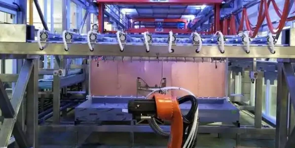
At APTPCB, we review hundreds of EV designs annually. The transition from a CAD file to a physical board is where most risks can be mitigated. We recommend a structured checkpoint system during the design phase.
Checkpoint 1: Creepage and Clearance Verification
- Recommendation: Use the UL 840 or IEC 60664-1 standards to calculate required spacing based on your pollution degree and voltage.
- Risk: Arcing between traces.
- Acceptance: Automated DRC (Design Rule Check) set to high-voltage constraints, followed by manual review.
Checkpoint 2: Thermal Via Design
- Recommendation: For power components, place thermal vias directly in the pad. Use plugged and capped vias (VIPPO) if soldering requires it, or open vias if solder wicking is managed.
- Risk: Components overheating due to poor heat transfer to inner layers.
- Acceptance: Thermal simulation showing junction temperatures remain within safe limits.
Checkpoint 3: Heavy Copper Etching Compensation
- Recommendation: When using Heavy Copper PCB (e.g., 4 oz+), increase the spacing between traces. Etching thick copper results in a trapezoidal trace shape, reducing the effective air gap.
- Risk: Short circuits or failing electrical clearance tests.
- Acceptance: Consult the manufacturer's DFM guidelines for minimum spacing based on copper weight.
Checkpoint 4: Solder Mask Selection
- Recommendation: Use high-quality, high-voltage rated solder mask. Ensure the mask dams between pads are sufficient to prevent solder bridging.
- Risk: Solder bridges on fine-pitch high-voltage pins.
- Acceptance: Verify minimum solder dam width (typically 4 mil) is maintainable.
Checkpoint 5: Layer Stackup Balance
- Recommendation: Ensure a symmetrical stackup to prevent warping. EV boards often have heavy copper on internal layers; if unbalanced, the board will bow during reflow.
- Risk: Board warping causes assembly defects or inability to fit in the housing.
- Acceptance: Review stackup with the fab house before freezing the design.
Checkpoint 6: High-Current Path Optimization
- Recommendation: Avoid right angles on high-current traces. Use polygons/planes rather than thin traces.
- Risk: Current crowding at corners creates hot spots (current density issues).
- Acceptance: Current density simulation.
Checkpoint 7: Surface Finish Selection
- Recommendation: ENIG (Electroless Nickel Immersion Gold) is preferred for flat surfaces (good for fine pitch) and corrosion resistance. HASL is acceptable for simple designs but less planar.
- Risk: Poor solder joints on complex components.
- Acceptance: Specify finish based on assembly requirements.
Checkpoint 8: Final DFM Review
- Recommendation: Submit data for a comprehensive DFM Guideline check before production.
- Risk: Production delays due to "on-hold" engineering queries.
- Acceptance: Clean DFM report from the manufacturer.
Electric Vehicle (EV) Charger PCB common mistakes (and the correct approach)
Even with a solid plan, specific pitfalls can derail production or cause field failures. Here are the most frequent errors we see in EV Charger PCB designs.
1. Underestimating Thermal Expansion (CTE Mismatch)
- The Mistake: Using standard FR4 with large ceramic components or heavy copper without considering Z-axis expansion.
- The Consequence: Plated through-holes (PTH) crack or separate from internal layers during thermal cycling.
- The Fix: Use High-Tg materials and materials with lower CTE (Coefficient of Thermal Expansion) to match component stress.
2. Insufficient Isolation Slots
- The Mistake: Relying solely on solder mask for high-voltage isolation. Solder mask is not considered a reliable insulator by safety standards like UL.
- The Consequence: Safety certification failure.
- The Fix: Add physical milled slots (air gaps) between high-voltage primary and low-voltage secondary sides.
3. Ignoring Pollution Degree
- The Mistake: Designing for a clean lab environment (Pollution Degree 1) when the charger will be outside (Pollution Degree 3).
- The Consequence: Dust and moisture accumulation lead to tracking and short circuits.
- The Fix: Design spacing rules for Pollution Degree 3 and apply conformal coating.
4. Poor Connector Placement
- The Mistake: Placing high-force connectors (for charging cables) in the center of the board without mechanical support.
- The Consequence: Board flexing cracks solder joints or traces.
- The Fix: Place connectors near mounting holes or board edges and use additional mechanical retention.
5. Neglecting In-Circuit Test (ICT) Points
- The Mistake: Designing a dense board without test points for mass production validation.
- The Consequence: Inability to efficiently test boards on the assembly line.
- The Fix: Include test pads on a single side of the PCB for pogo-pin fixtures.
6. Overlooking Copper Balance
- The Mistake: Large copper planes on one side and sparse traces on the other.
- The Consequence: Severe warping ("potato chipping") during reflow soldering.
- The Fix: Use copper thieving (hatching) in empty areas to balance the copper distribution.
Electric Vehicle (EV) Charger PCB FAQ (cost, lead time, ave observed that the most successful projects prioritize Design for Manufacturing (DFM) files, stackup, impedance, IPC class)
To clarify any remaining uncertainties, here are the most frequent questions engineers ask regarding EV Charger PCB manufacturing.
Q: Can I use standard FR4 for an EV charger? A: For low-power Level 1 chargers, yes. However, for Level 2 and DC Fast Chargers, you typically need High-Tg FR4 (Tg >170°C) and High CTI (>600V) materials to ensure safety and reliability.
Q: What is the best surface finish for EV PCBs? A: ENIG is generally preferred because it offers a flat surface for component placement and excellent corrosion resistance. Immersion Silver is also used in some automotive applications but requires careful handling.
Q: How thick should the copper be? A: It depends on the current. Control boards use standard 1 oz. Power boards often use 3 oz, 4 oz, or even 6 oz copper. For extremely high currents, busbars or Metal Core PCBs are used.
Q: Do I need UL certification for the PCB? A: Yes. The bare PCB must have a UL 94 V-0 flammability rating. Furthermore, the entire charger assembly will likely need UL/CE certification, which requires the PCB to meet specific spacing and material standards.
Q: What is the difference between an EV Converter PCB and an EV Controller PCB? A: The EV Converter PCB handles the high-power conversion (AC-DC or DC-DC) and deals with high voltage/current. The EV Controller PCB handles the logic, communication, and user interface, operating at low voltages (5V, 12V).
Q: Why is CTI important? A: CTI (Comparative Tracking Index) measures how easily a material conducts electricity across its surface when contaminated. High voltage + outdoor contaminants = high risk of arcing. High CTI materials resist this.
Q: How do you test these boards? A: Beyond standard E-Test (Open/Short), EV boards often undergo Hi-Pot testing (high voltage isolation), Impedance Control testing (for comms), and Thermal Stress testing.
Q: What is the lead time for EV Charger PCBs? A: Prototypes can be done in 24-48 hours. Mass production typically takes 2-4 weeks depending on material availability (especially for heavy copper or specialized laminates).
Electric Vehicle (EV) Charger PCB glossary (key terms)
Finally, let's define the technical vocabulary used throughout this guide to ensure clarity in your specifications.
| Term | Definition |
|---|---|
| BMS | Battery Management System. The electronic system that manages a rechargeable battery (cell balancing, monitoring). |
| Creepage | The shortest distance between two conductive parts along the surface of the insulation. |
| Clearance | The shortest distance between two conductive parts through the air. |
| CTI | Comparative Tracking Index. A measure of the electrical breakdown (tracking) properties of an insulating material. |
| EVSE | Electric Vehicle Supply Equipment. The technical term for the charging station/infrastructure. |
| Heavy Copper | PCBs with copper thickness generally greater than 3 oz (105µm) per square foot. |
| Hi-Pot Test | High Potential Test. Verifies the insulation capability of the PCB by applying high voltage. |
| IATF 16949 | The international standard for automotive quality management systems. |
| OBC | On-Board Charger. The device inside the vehicle that converts AC grid power to DC for the battery. |
| Pollution Degree | A classification of the environmental conditions (dust, moisture) the equipment will face. |
| Tg | Glass Transition Temperature. The point where the PCB substrate transitions from a rigid to a deformable state. |
| Thermal Vias | Plated holes designed specifically to transfer heat from one layer of the PCB to another (usually to a ground plane). |
| V-0 | A UL 94 flammability standard indicating that the material stops burning within 10 seconds on a vertical specimen. |
Conclusion (next steps)
The EV Charger PCB is the backbone of the electric mobility revolution. Whether you are designing a compact home controller or a high-power DC converter, the principles remain the same: prioritize safety through spacing, manage heat through material selection, and validate reliability through rigorous testing.
Success in this field requires more than just a schematic; it requires a manufacturing strategy that accounts for the harsh realities of high-voltage electronics.
Ready to move from concept to production? At APTPCB, we specialize in automotive and high-power PCB fabrication. To get an accurate quote and a complimentary DFM review, please prepare the following:
- Gerber Files: RS-274X format.
- Stackup Details: Desired layer count and copper weight.
- Material Specs: Tg requirement and CTI value.
- Test Requirements: Specific Hi-Pot or impedance constraints.
Contact our engineering team today to ensure your EV infrastructure is built on a foundation of quality.