Contents
- Highlights
- Fast Turn PCB: Definition and Scope
- Fast Turn PCB Rules and Specifications
- Fast Turn PCB Implementation Steps
- Fast Turn PCB Troubleshooting
- 6 Essential Rules for Fast Turn PCB (Cheat Sheet)
- FAQ
- Request a Quote / DFM Review for Fast Turn PCB
- Conclusion
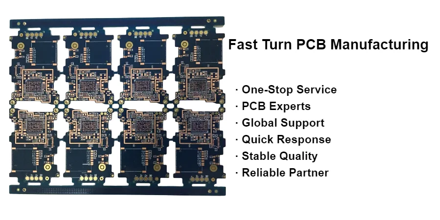
In the electronics hardware development cycle, time is often the most expensive currency. Fast turn pcb (Fast Turnaround Printed Circuit Board) manufacturing is the specialized service of fabricating bare boards in accelerated timeframes—typically ranging from 24 hours to 72 hours—to support rapid prototyping, NPI (New Product Introduction), and emergency repairs. Unlike standard production, which optimizes for panel utilization and cost efficiency over 1-2 weeks, fast turn fabrication prioritizes speed, dedicated tooling, and immediate line capacity.
However, "fast" does not mean "loose" with engineering rules. In fact, requesting a 24-hour turnaround requires stricter adherence to DFM (Design for Manufacturing) guidelines than standard production. If a design contains ambiguous data or pushes the limits of physics (e.g., trace widths below 3 mil on a rush order), the resulting Engineering Questions (EQ) can halt production, negating the premium paid for speed. As Senior CAM Engineers at APTPCB, we see that successful fast turn projects are those that balance design complexity with manufacturing readiness.
Quick Answer
For engineers seeking immediate results, fast turn pcb relies on using standard materials and robust design tolerances to minimize processing time.
- Standard Rule: Stick to standard FR4 materials (TG150/TG170) and copper weights (1oz/H oz) available in stock.
- Critical Pitfall: Submitting files with "netlist violations" or ambiguous layer stackups. A single EQ email can delay a 24-hour job by a full day if the designer is in a different time zone.
- Verification: Always run a DFM check (or use our online Gerber viewer) to ensure drill files match the drill chart and annular rings are sufficient (≥4mil).
- Layer Count: 2-6 layers are ideal for 24-48 hour turns; 8+ layers or HDI typically require 72+ hours due to lamination cycles.
- Surface Finish: ENIG and HASL are the fastest; Hard Gold or ENEPIG add processing steps.
Highlights
- Speed vs. Specs: The tighter the tolerances (e.g., impedance control ±5%), the higher the risk of yield loss, which is catastrophic for a 24-hour turn.
- Material Availability: Fast turn relies on "in-stock" laminates. Specifying exotic Rogers or Arlon materials without checking stock first is the #1 cause of delays.
- Data Integrity: ODB++ is preferred over Gerbers for fast turn because it integrates the netlist and stackup, reducing CAM setup time.
- Drill Tech: Mechanical drilling is faster for standard vias; laser drilling (HDI) adds significant time for microvia formation and plating.
- Solder Mask: Green is the standard "fast" color because it cures the fastest and is always on the coating line.
Fast Turn PCB: Definition and Scope
When we discuss fast turn pcb, we are referring to a manufacturing workflow designed to bypass the queue of standard production. In a standard flow, orders are batched to maximize panel usage (pooling). In a fast turn flow, your board often gets its own panel or priority placement.
The scope of fast turn capabilities at APTPCB generally covers:
- 24-Hour Turn: Double-sided (2L) and simple Multilayer (4L-6L) boards. Requires standard FR4, standard specs (track/space ≥ 5mil), and immediate data approval.
- 48-72 Hour Turn: Higher layer counts (8L-12L), simple Rigid-Flex, or boards requiring impedance control.
- Expedited Production: For larger volumes (small batch) that need to be finished in 5-7 days rather than the standard 15.
It is crucial to understand that "Fast Turn" implies a trade-off. You are trading cost (paying a premium) for time. To maximize this trade-off, the design must be "CAM-ready." If the CAM engineer has to manually repair slivers or ask about a missing drill file, the "Fast Turn" clock stops.
For complex technologies like HDI PCB or Rigid-Flex PCB, "Fast Turn" might mean 5 days instead of 20. The physics of sequential lamination, laser drilling, and plasma cleaning cannot be rushed beyond a certain point without compromising reliability.
Tech / Decision Lever → Practical Impact
| Decision Lever / Spec | Practical Impact (Yield/Cost/Reliability) |
|---|---|
| Material Selection (FR4 vs. Exotic) | Standard FR4 is always in stock for 24h turns. Exotic materials (Rogers/Teflon) may require procurement lead time (days/weeks). |
| Via Technology (Through vs. Blind/Buried) | Through-holes are drilled in one pass. Blind/Buried vias require sequential lamination cycles, adding 24-48 hours per cycle. |
| Surface Finish (ENIG vs. Hard Gold) | ENIG/HASL are continuous processes. Hard Gold requires selective plating and taping, adding manual labor and time. |
| Solder Mask Color (Green vs. White/Black) | Green cures fastest and is the default line configuration. Black/White require higher exposure energy and longer oven times. |
Fast Turn PCB Rules and Specifications
To ensure your board flies through the factory without hitting a "CAM Hold," adhere to these specifications. These values are optimized for speed and yield.
| Rule | Recommended Value | Why it matters | How to verify |
|---|---|---|---|
| Min Trace / Space | 5mil / 5mil (0.127mm) | Tighter spacing (3mil) requires slower etching and stricter AOI, increasing risk of shorts/opens. | Use CAD DRC (Design Rule Check) set to 5mil minimum. |
| Min Mechanical Drill | 0.25mm (10mil) | Smaller drills (0.15mm) break more often and have lower aspect ratio limits for plating. | Check NC Drill file or Drill Table in Fab Drawing. |
| Annular Ring | ≥ 4mil (pad vs hole) | Allows for slight drill wander without breaking the connection (breakout). Vital for rapid registration. | Visual check in Gerber Viewer: Pad diameter - Hole diameter ≥ 8mil. |
| Solder Mask Dam | ≥ 4mil | Prevents solder bridging during assembly. Smaller dams may peel off during development. | Measure the mask web between pads in CAM software. |
| Copper Weight | 1 oz (35µm) | Heavier copper (2oz+) takes longer to etch and requires wider spacing rules. | Specify in stackup notes. |
| Aspect Ratio | 8:1 | High aspect ratios (thick board, small hole) are hard to plate quickly and reliably. | Board Thickness / Smallest Drill Diameter. |
Fast Turn PCB Implementation Steps
Executing a fast turn order requires synchronization between the designer and the manufacturer. Follow this process to ensure zero delays.
Implementation Process
Step-by-step execution guide
Export data in Gerber X2 or ODB++ format. Ensure the drill file (NC Drill) is included and matches the drill chart. Include a clear text file with stackup requirements (Layer 1 = Top, etc.).
Before submitting the order, confirm with the vendor that the specific laminate (e.g., Isola 370HR) and copper thickness are in stock. For 24h turns, use "Standard Stock" options.
Stay glued to your email for the first 2-4 hours after submission. This is when CAM engineers review files. Unanswered Engineering Questions (EQs) are the #1 cause of missed deadlines.
Select "Priority" shipping (DHL/FedEx/UPS). Ensure the commercial invoice is accurate to prevent customs delays. A board finished in 24 hours is useless if it sits in customs for 3 days.
Fast Turn PCB Troubleshooting
Even with the best intentions, fast turn projects can face hurdles. Here are common failure modes and how to fix them.
1. The "Missing Drill" Error
Often, designers export Gerbers but forget the NC Drill file, or the drill file is not in the same units (Imperial vs. Metric) as the Gerbers.
- Fix: Use ODB++ if possible. If using Gerbers, open them in a viewer to ensure holes align with pads.
2. Ambiguous Stackup
Sending a 4-layer board without specifying the layer order (e.g., is "GND" layer 2 or 3?) forces the CAM engineer to stop and ask.
- Fix: Name files clearly:
L1_Top.gbr,L2_GND.gbr,L3_PWR.gbr,L4_Bot.gbr. Include a simple README.txt.
3. Impedance Mismatch
Designers often request specific impedance (e.g., 50Ω) but use trace widths calculated for a different material dielectric constant (Dk).
- Fix: Use the manufacturer's impedance calculator or specify "Impedance controlled: Adjust trace width as needed to meet 50Ω." This gives the CAM engineer permission to modify traces slightly without stopping for approval.
4. Slivers and Acid Traps
Acute angles in copper traces can trap acid during etching, causing over-etching (opens).
- Fix: Ensure all trace intersections are T-junctions or >90 degrees. Avoid acute angles.

6 Essential Rules for Fast Turn PCB (Cheat Sheet)
| Rule / Guideline | Why It Matters (Physics/Cost) | Target Value / Action |
|---|---|---|
| Standard Material (FR4) | Non-standard materials require ordering time. FR4 is always on the shelf. | TG150 / TG170 |
| Trace / Space | Tight spacing slows down etching and AOI inspection. | ≥ 5mil / 5mil |
| Minimum Drill Size | Micro-drills break easily and limit stack height (aspect ratio). | ≥ 0.2mm (8mil) |
| Surface Finish | Complex finishes (Hard Gold, ENEPIG) add process steps. | ENIG or HASL |
| Silkscreen Legibility | Small text blurs; illegible text triggers quality holds. | Height ≥ 30mil, Line ≥ 5mil |
| Data Format | Reduces interpretation errors and CAM setup time. | ODB++ or Gerber X2 |
FAQ
Q: Does "Fast Turn" include shipping time?
A: No. The turnaround time (e.g., 24 hours) refers to the manufacturing time inside the factory. Shipping (DHL/FedEx) typically adds 1-3 days depending on your location.
Q: Can I get HDI boards on a 24-hour turn?
A: Generally, no. HDI PCB requires laser drilling and sequential lamination cycles. A simple 1+N+1 HDI board usually takes a minimum of 3-4 days. 24-hour turns are best suited for standard through-hole technology.
Q: Is electrical testing included in fast turn orders?
A: Yes, at APTPCB, 100% Flying Probe testing is standard for all prototype and fast turn orders to ensure no opens or shorts. We do not skip quality checks for speed.
Q: How much more does fast turn cost?
A: Expect a premium of 30% to 100% over standard lead times, depending on the urgency (24h vs 72h). This covers the cost of disrupting the standard production queue and dedicated engineering resources.
Q: What happens if my design fails the DFM check?
A: The clock stops. We will issue an EQ (Engineering Question). The turnaround time resets or pauses until we receive your clarified data or approval to proceed with modifications.
Request a Quote / DFM Review for Fast Turn PCB
Ready to expedite your project? To get the fastest accurate quote and start production immediately, please provide:
- Gerber Files: RS-274X or ODB++ format (preferred).
- Quantity: Prototype quantities (e.g., 5, 10, 50 pcs).
- Turn Time Required: Specify 24h, 48h, or Standard.
- Stackup Details: Copper weight, board thickness (e.g., 1.6mm), and layer count.
- Material: Confirm FR4 TG value (e.g., TG150).
Submit your files via our Quote Page for an instant review.
Conclusion
Fast turn pcb fabrication is a powerful tool for agile hardware development, allowing engineers to iterate designs in days rather than weeks. However, speed is a collaborative effort. By adhering to standard materials, robust design rules (5mil trace/space), and clear data documentation, you empower the CAM team to process your board without delays. Remember: the fastest board is the one that passes DFM on the first pass.
Signed, The Engineering Team at APTPCB