Definition, scope, and who this guide is for
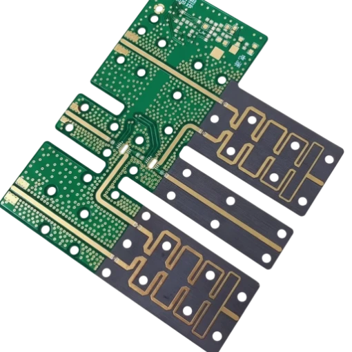
Fire Control Radar (FCR) represents the highest tier of precision in radio frequency detection systems. Unlike search radars that scan wide volumes of airspace to detect presence, a Fire Control Radar is designed to lock onto a specific target, continuously track its trajectory, and provide guidance data to a weapon system. The printed circuit boards (PCBs) inside these units function as the critical interface between high-frequency analog signals and digital processing, often operating in X-band, Ku-band, or Ka-band frequencies.
This guide is written for systems engineers, hardware designers, and procurement leads responsible for sourcing PCBs for tracking and guidance systems. It moves beyond basic datasheet parameters to address the manufacturability, reliability, and supply chain stability required for defense and high-end industrial applications. Whether you are developing an airborne AESA Radar PCB or a land-based tracking unit, the physical realization of the circuit determines the system's accuracy.
At APTPCB (APTPCB PCB Factory), we understand that the margin for error in these systems is non-existent. A minor impedance mismatch or a slight variation in dielectric constant can result in phase errors that degrade the radar's ability to resolve a target. This playbook outlines the specific engineering decisions, risk mitigation strategies, and validation protocols necessary to move a Fire Control Radar design from prototype to production without compromising performance.
When to use Fire Control Radar (and when a standard approach is better)
Understanding the operational context of your radar system dictates the complexity of the PCB fabrication process; while standard surveillance requires coverage, Fire Control Radar demands precision.
Use Fire Control Radar specifications when:
- Target Lock is Required: The system must maintain a continuous track on a fast-moving object with high update rates.
- Phase Stability is Critical: You are designing a phased array or AESA system where beamforming relies on precise phase relationships between antenna elements.
- Operating Frequency is High: The application operates in X-band (8-12 GHz) or higher, where standard FR4 materials cause unacceptable signal loss.
- Thermal Density is High: The system uses Gallium Nitride (GaN) amplifiers that generate significant heat in a small footprint, requiring advanced thermal management like metal-core or coin-insertion PCBs.
- Environment is Harsh: The unit will be deployed in high-vibration (airborne/missile) or extreme temperature environments.
Opt for a standard surveillance or GPR Radar PCB approach when:
- Application is General Detection: You only need to know if an object is present, not its exact firing solution coordinates.
- Frequency is Low: The system operates in L-band or S-band where standard high-Tg FR4 or mid-performance laminates suffice.
- Budget is Constrained: The cost of PTFE-based laminates and controlled depth drilling is not justifiable for the application's performance needs.
- Latency is Tolerable: The system does not require real-time, millisecond-level loop closure for guidance.
Fire Control Radar specifications (materials, stackup, tolerances)
Once you have determined that your project requires the precision of a Fire Control Radar, the next step is defining the rigid specifications that will govern manufacturing.
- Base Material Selection:
- Use high-frequency laminates with extremely low dielectric loss (Df < 0.0025). Common choices include Rogers RO4350B, RO3003, or Taconic TLY series.
- Ensure the Dielectric Constant (Dk) tolerance is within ±0.05 to maintain impedance control at high frequencies.
- Hybrid Stackup Configuration:
- Combine expensive RF materials on signal layers with standard high-Tg FR4 on digital/power layers to optimize cost and structural integrity.
- Use specific prepregs that are compatible with both material types to prevent delamination during lamination cycles.
- Copper Surface Roughness:
- Specify VLP (Very Low Profile) or HVLP (Hyper Very Low Profile) copper foil. At millimeter-wave frequencies, skin effect makes surface roughness a significant contributor to insertion loss.
- Trace Width and Spacing Tolerances:
- Require ±0.5 mil (±12.7 µm) or better for RF signal traces. Standard ±10% tolerances are often insufficient for impedance-matched lines in Ku-band or Ka-band.
- Via Structure and Plating:
- Implement blind and buried vias to reduce signal stubs that cause reflections.
- For AESA Radar PCB designs, specify copper-filled stacked microvias to maximize density and thermal conductivity.
- Surface Finish:
- Immersion Silver or ENEPIG (Electroless Nickel Electroless Palladium Immersion Gold) are preferred. They provide a flat surface for component mounting and do not have the magnetic nickel skin effect losses associated with standard ENIG at very high frequencies.
- Thermal Management:
- Embed copper coins or use heavy copper (2oz+) on inner layers for heat dissipation from power amplifiers.
- Thermal conductivity of the dielectric material should be considered; ceramic-filled PTFE often offers better thermal performance than pure PTFE.
- Layer Registration:
- Target layer-to-layer registration of ±3 mils or better. Misalignment in coupled lines or antenna patches can skew the radiation pattern.
- Solder Mask:
- Use LPI (Liquid Photoimageable) solder mask with strict thickness control. In some RF sections, solder mask should be removed entirely (solder mask defined pads vs. non-solder mask defined) to prevent dielectric loading.
- Impedance Control:
- Specify 50Ω single-ended and 100Ω differential pairs with a tolerance of ±5% rather than the standard ±10%.
- Cleanliness and Ionic Contamination:
- Require ionic contamination testing results below 1.56 µg/cm² NaCl equivalent. Residues can cause electrochemical migration or leakage in sensitive high-impedance circuits.
Fire Control Radar manufacturing risks (root causes and prevention)
High-performance specifications introduce specific manufacturing risks that can lead to latent failures in the field; understanding these root causes allows for proactive prevention.
- Risk: Phase Instability
- Root Cause: Variations in dielectric constant (Dk) across the PCB panel or inconsistent etching of trace widths.
- Detection: TDR (Time Domain Reflectometry) and VNA (Vector Network Analyzer) testing on coupons.
- Prevention: Use "rolled" copper foil for consistency and specify Dk-controlled laminate batches from the material supplier.
- Risk: Delamination in Hybrid Stackups
- Root Cause: Mismatched Coefficient of Thermal Expansion (CTE) between PTFE-based RF layers and FR4 digital layers during reflow.
- Detection: Thermal stress testing (solder float) and microsection analysis.
- Prevention: Select prepregs with cure temperatures and CTEs that bridge the gap between the dissimilar core materials.
- Risk: Plating Voids in High Aspect Ratio Vias
- Root Cause: Inadequate plating solution flow into deep, narrow vias (aspect ratio > 10:1).
- Detection: Cross-section analysis and electrical continuity testing.
- Prevention: Utilize pulse plating technology and specify a maximum aspect ratio compatible with the manufacturer's capability.
- Risk: Passive Intermodulation (PIM)
- Root Cause: Microscopic contaminants, rough copper, or ferromagnetic materials (like Nickel in ENIG) in the signal path.
- Detection: PIM testing equipment.
- Prevention: Use non-magnetic surface finishes (Immersion Silver) and ensure strict chemical cleaning processes.
- Risk: Dimensional Instability of PTFE
- Root Cause: PTFE is soft and can deform mechanically during drilling or routing.
- Detection: CMM (Coordinate Measuring Machine) inspection of feature locations.
- Prevention: Use ceramic-filled PTFE composites which are mechanically more stable than pure PTFE.
- Risk: Thermal Runaway
- Root Cause: Insufficient heat transfer from GaN chips through the PCB to the heatsink.
- Detection: Thermal imaging during power-up testing.
- Prevention: Implement dense thermal via arrays or embedded copper coins directly under hot components.
- Risk: Solder Mask Effect on Impedance
- Root Cause: Solder mask adds a dielectric layer on top of traces, lowering impedance and increasing loss.
- Detection: Impedance testing post-solder mask application.
- Prevention: Account for solder mask in the initial stackup calculation or remove mask from critical RF traces.
- Risk: Moisture Absorption
- Root Cause: Some laminate materials absorb moisture over time, changing Dk and Df.
- Detection: Humidity testing.
- Prevention: Bake boards before assembly and store in vacuum-sealed packages with desiccants.
Fire Control Radar validation and acceptance (tests and pass criteria)

To ensure the manufactured PCBs meet the stringent requirements of a Fire Control Radar system, a robust validation plan with clear pass/fail criteria is essential.
- Microsection Analysis:
- Objective: Verify internal stackup, plating thickness, and via quality.
- Method: Cross-sectioning of quality coupons from the panel edge.
- Criteria: Copper thickness meets IPC Class 3 (e.g., average 25µm in hole); no knee cracks; dielectric thickness within ±10%.
- Impedance Verification:
- Objective: Confirm signal integrity parameters.
- Method: TDR testing on test coupons representing critical traces.
- Criteria: Measured impedance must be within ±5% of the design value (e.g., 50Ω ± 2.5Ω).
- Thermal Stress Test:
- Objective: Ensure structural integrity under soldering heat.
- Method: Solder float test at 288°C for 10 seconds (repeated cycles).
- Criteria: No delamination, blistering, or pad lifting visible under 10x magnification.
- Ionic Contamination Test:
- Objective: Prevent corrosion and electrical leakage.
- Method: ROSE (Resistivity of Solvent Extract) testing.
- Criteria: Contamination levels < 1.56 µg/cm² NaCl equivalent.
- Solderability Test:
- Objective: Ensure pads will accept solder reliably during assembly.
- Method: Dip and look or wetting balance test.
- Criteria: >95% coverage of the pad with a smooth, continuous solder coating.
- Dimensional Inspection:
- Objective: Verify mechanical fit and antenna patch dimensions.
- Method: CMM or optical measurement.
- Criteria: Dimensions within specified tolerances (typically ±0.1mm for outline, tighter for RF features).
- Electrical Continuity and Isolation:
- Objective: Detect opens and shorts.
- Method: Flying probe or bed-of-nails testing at high voltage.
- Criteria: 100% pass; isolation resistance > 100 MΩ.
- Intermodulation Testing (Optional but Recommended):
- Objective: Verify low PIM performance for high-power transmit paths.
- Method: Two-tone PIM test.
- Criteria: PIM products below -150 dBc (depending on system spec).
- Surface Finish Thickness Measurement:
- Objective: Ensure finish is thick enough for protection but thin enough for RF.
- Method: X-ray Fluorescence (XRF).
- Criteria: Immersion Silver thickness 0.15-0.4 µm; ENEPIG layers within spec.
Fire Control Radar supplier qualification checklist (RFQ, audit, traceability)
Selecting the right partner is as critical as the design itself. Use this checklist to vet potential suppliers for Fire Control Radar projects.
RFQ Inputs (What you must provide)
- Complete Gerber files (RS-274X or ODB++) with clear layer naming.
- Fabrication drawing specifying IPC Class 3 requirements.
- Material datasheet references (specific laminate series, not just "FR4").
- Stackup diagram with defined dielectric thicknesses and copper weights.
- Impedance control table linking trace widths/layers to target ohms.
- Drill chart distinguishing between plated and non-plated holes.
- Surface finish specification (e.g., Immersion Silver).
- Panelization requirements for assembly efficiency.
- Special requirements (e.g., edge plating, countersink, filled vias).
- Volume and lead time expectations (prototype vs. production).
Capability Proof (What they must demonstrate)
- Experience manufacturing hybrid (RF + FR4) stackups.
- Capability to handle soft PTFE materials without mechanical distortion.
- Equipment for ±5% impedance testing and reporting.
- Laser drilling capability for microvias (if HDI is used).
- Plasma etching capability for desmearing PTFE holes.
- Automated Optical Inspection (AOI) for inner and outer layers.
- X-ray inspection capability for registration verification.
- Controlled depth drilling/routing for cavity boards.
Quality System & Traceability (How they manage risk)
- ISO 9001 and AS9100 (Aerospace) certification.
- Material traceability system (can they trace a board back to the laminate lot?).
- UL certification for the specific stackup/material combination.
- Documented calibration schedule for test equipment (TDR, CMM).
- Process for handling Engineering Change Orders (ECOs).
- Statistical Process Control (SPC) implementation for key parameters.
Change Control & Delivery (How they ensure consistency)
- Policy on "No changes without prior approval" (critical for RF).
- Packaging standards (vacuum sealed, humidity indicator cards).
- First Article Inspection (FAI) report format.
- Disaster recovery plan for supply chain disruptions.
- History of on-time delivery performance.
- Technical support availability for DFM (Design for Manufacturing) reviews.
How to choose Fire Control Radar (trade-offs and decision rules)
Designing a Fire Control Radar involves balancing performance, cost, and manufacturability. Here are the key trade-offs to consider.
- Frequency vs. Material Cost:
- Rule: If operating below 2 GHz, standard FR4 may suffice. If operating > 5 GHz (C-band and up), you must choose PTFE or ceramic-filled hydrocarbon laminates. The material cost is higher, but signal integrity is non-negotiable.
- Hybrid vs. Pure RF Stackup:
- Rule: If the board has complex digital control logic and a simple RF front end, choose a Hybrid Stackup. It reduces cost by using FR4 for non-critical layers. If the entire board is high-frequency signal distribution, choose a Pure RF Stackup to avoid CTE mismatch issues.
- Surface Finish: ENIG vs. Immersion Silver:
- Rule: If shelf life and solderability are the only concerns, ENIG is standard. However, for Fire Control Radar, if insertion loss is critical, choose Immersion Silver or ENEPIG. The nickel layer in ENIG causes magnetic losses at high frequencies.
- HDI vs. Through-Hole:
- Rule: If you are designing a compact AESA Radar PCB with fine-pitch BGAs, choose HDI (High Density Interconnect). If space allows and component density is low, stick to Through-Hole to lower fabrication complexity and cost.
- Embedded Resistors vs. Discrete Components:
- Rule: If space is extremely limited and signal paths must be short, choose Embedded Passives. Otherwise, use Discrete Components for easier repair and lower board cost.
- Ground Radar PCB vs. Airborne:
- Rule: If the system is airborne, prioritize Weight and Vibration Resistance (thinner cores, flexible materials). If it is a Ground Radar PCB, prioritize Thermal Mass and Rigidity (thicker copper, metal cores).
Fire Control Radar FAQ (cost, lead time, Design for Manufacturability (DFM) files, materials, testing)
Q: How does the cost of a Fire Control Radar PCB compare to a standard PCB? A: Expect costs to be 3x to 10x higher than standard FR4 boards. This premium is driven by expensive RF laminates (Rogers/Taconic), complex hybrid lamination cycles, tighter tolerance requirements (±5% impedance), and rigorous IPC Class 3 testing.
Q: What is the typical lead time for manufacturing Fire Control Radar PCBs? A: Standard lead time is 15-20 working days. Quick-turn options (5-10 days) are possible but depend on material availability; specialized RF laminates often have long procurement lead times if not in stock.
Q: What specific DFM files are needed for a Fire Control Radar quote? A: Beyond standard Gerbers, you must provide a detailed stackup drawing specifying the exact material types (e.g., Rogers RO4350B 10mil), a drill chart with aspect ratios, and an impedance table. 3D STEP files are helpful for verifying cavity or heatsink fitment.
Q: Can I use standard FR4 for the digital section of a Fire Control Radar? A: Yes, this is the standard "hybrid stackup" approach. It significantly reduces cost and improves mechanical rigidity. However, the manufacturer must be experienced in bonding FR4 and PTFE materials together to prevent delamination.
Q: What testing is mandatory for Fire Control Radar acceptance criteria? A: Mandatory tests typically include 100% electrical continuity, TDR impedance testing on coupons, microsection analysis for plating quality, and ionic contamination testing. High-reliability orders may also require thermal shock or burn-in testing.
Q: How do I choose between Rogers and Taconic materials for my Radar PCB? A: Both offer excellent high-frequency performance. The choice often comes down to availability and specific Dk/Df needs. Rogers RO4000 series is popular for its processability similar to FR4, while Taconic offers specialized PTFE options for specific microwave applications.
Q: What is the impact of copper roughness on Fire Control Radar performance? A: At frequencies above 10 GHz, rough copper increases the effective resistance due to the skin effect, leading to higher insertion loss. Specifying VLP (Very Low Profile) or HVLP copper is crucial for maintaining signal strength.
Q: Is a Doppler Radar PCB different from a Fire Control Radar PCB? A: Doppler radar focuses on velocity measurement and can be simple (like automatic door openers). Fire Control Radar often includes Doppler processing but adds precise tracking and guidance capabilities, requiring much tighter PCB specifications and reliability standards.
Resources for Fire Control Radar (related pages and tools)
- Aerospace & Defense PCB Solutions – Explore our specific capabilities and certifications for defense-grade electronics manufacturing.
- High-Frequency PCB Manufacturing – Deep dive into the processing of RF materials and the technical nuances of high-speed signal integrity.
- Rogers PCB Material Guide – Understand the specific properties of Rogers laminates and why they are the industry standard for radar applications.
- HDI PCB Technology – Learn how High Density Interconnect technology enables the miniaturization required for modern AESA radar modules.
- Microwave PCB Capabilities – Review our technical parameters for microwave circuits, including tolerance and surface finish options.
Request a quote for Fire Control Radar (Design for Manufacturability (DFM) review + pricing)
Ready to move your design to production? APTPCB provides a comprehensive DFM review to identify potential signal integrity or manufacturability issues before you commit to fabrication.
Get a Quote for Your Fire Control Radar Project
For the most accurate DFM and pricing, please include:
- Gerber Files: RS-274X or ODB++ format.
- Stackup Details: Specific material requirements (e.g., Rogers 4350B) and layer order.
- Fabrication Drawing: Including tolerances, drill chart, and IPC class.
- Test Requirements: Impedance specs, TDR points, and any special validation needs.
- Volume: Prototype quantity and estimated production volume.
Conclusion (next steps)
Fire Control Radar systems demand a manufacturing partner who treats every micron of tolerance as a critical mission parameter. From selecting the right low-loss materials to executing a flawless hybrid stackup, the PCB is the foundation of your system's tracking accuracy. By following the specifications, risk mitigation strategies, and validation steps outlined in this playbook, you can ensure your radar hardware performs reliably in the field. When you are ready to validate your design or scale production, our engineering team is here to support your mission-critical requirements.