Quick Answer (30 seconds)
A robust first article inspection (fai) for pcba: checklist ensures that the manufacturing process is correctly calibrated before volume production begins. This validation step prevents systemic defects like wrong component placement, reflow issues, or BOM mismatches.
- Verify BOM Match: Confirm every installed component matches the Manufacturer Part Number (MPN) and value in the Bill of Materials.
- Check Polarity: Inspect all diodes, ICs, and electrolytic capacitors for correct orientation relative to the silkscreen.
- Solder Quality: Validate fillets against IPC-A-610 (Class 2 or 3) standards; look for wetting, bridges, or cold joints.
- Hidden Joints: Use X-ray to inspect BGAs and QFNs, ensuring voiding is within acceptable limits (typically <25%).
- First Power-Up: Measure resistance on power rails to ground before applying voltage to prevent catastrophic shorts.
- Documentation: Record all measurements and visual evidence in a formal FAI report for traceability.
When first article inspection (fai) for pcba: checklist applies (and when it doesn’t)
Understanding when to trigger a full FAI process saves time while maintaining quality control.
When it applies:
- New Product Introduction (NPI): The very first run of a new design requires a complete validation of the assembly process.
- Design Revisions: Any change to the copper layout, BOM components, or stencil design necessitates a new FAI.
- Process Changes: If the assembly line moves to a new machine or changes solder paste chemistry, the first output must be verified.
- Long Gaps in Production: Resuming manufacturing after a hiatus (e.g., >12 months) often triggers a re-validation to ensure machine settings remain valid.
- Supplier Changes: Switching PCB fabricators or assembly houses requires a new first article to verify their specific capabilities.
When it doesn’t apply:
- Continuous Production: During a stable volume run, statistical process control (SPC) and sampling are used instead of full FAI on every board.
- Minor Non-Critical Substitutions: Replacing a passive resistor with an identical spec from a different approved vendor (AVL) may not require a full FAI if the form factor is identical.
- Bare Board Fabrication: While bare boards undergo their own inspection, the first article inspection (fai) for pcba: checklist specifically targets the assembled state, not just the substrate.
- Firmware Updates Only: If the hardware remains unchanged and only software is flashed, a hardware FAI is unnecessary (though functional testing is still required).
Rules & specifications

A strict set of rules defines the pass/fail criteria for the first article. These parameters ensure the board meets reliability standards before the rest of the batch is processed.
| Rule | Recommended Value/Range | Why it matters | How to verify | If ignored |
|---|---|---|---|---|
| Component Presence | 100% match to BOM | Missing parts break functionality immediately. | Visual inspection or AOI comparison. | Board fails functional test; costly rework. |
| Polarity/Orientation | Match silkscreen/assembly drawing | Reversed capacitors explode; reversed ICs burn out. | Visual check of Pin 1 markers. | Catastrophic failure upon power-up. |
| Solder Fillet Shape | Concave meniscus | Indicates proper wetting and strong mechanical bond. | Microscope (45° angle) or AOI. | Weak joints crack under thermal cycling. |
| BGA Voiding | < 25% of ball area (IPC Class 2) | Excessive voids increase thermal resistance and weaken joints. | X-ray inspection (2D or 3D). | Intermittent connection failures in field. |
| Solder Bridging | 0 shorts allowed | Connects unrelated nets, causing malfunctions. | Electrical test or magnified visual check. | Short circuits; potential component damage. |
| Component Alignment | < 50% pad overhang allowed | Misalignment reduces contact area and reliability. | AOI or high-mag microscope. | Tombstoning or weak electrical contact. |
| Solder Balling | None > 0.13mm (loose) | Loose balls can dislodge and cause shorts later. | Visual inspection after wash. | Random shorts during vibration/operation. |
| Through-Hole Fill | > 75% vertical fill (Class 2) | Ensures mechanical strength for connectors/leads. | X-ray or cross-section analysis. | Connector leads pull out under stress. |
| Cleanliness (Flux) | < 1.56 µg/cm² NaCl equiv. | Corrosive residues degrade circuits over time. | ROSE test or Ion Chromatography. | Dendritic growth and leakage currents. |
| PCB Warpage | < 0.75% of diagonal | Excessive bow stresses solder joints and components. | Flat table measurement with gauge. | Cracks in MLCCs or BGA solder balls. |
Implementation steps
Executing a first article inspection (fai) for pcba: checklist requires a systematic approach. APTPCB (APTPCB PCB Factory) recommends following these sequential steps to catch errors early.
BOM and Data Verification
- Action: Compare the received components against the approved Bill of Materials (BOM) and Gerber files.
- Key Parameter: Manufacturer Part Number (MPN) and quantity.
- Acceptance: 100% match; no unapproved substitutes.
Solder Paste Inspection (SPI)
- Action: Measure solder paste volume and height on the bare PCB before component placement.
- Key Parameter: Paste height (typically 100-150µm depending on stencil).
- Acceptance: Volume within ±50% of aperture target; no bridging.
First Board Mounting & Reflow
- Action: Run a single PCB through the pick-and-place machine and reflow oven.
- Key Parameter: Reflow profile (Time Above Liquidus: 60-90s).
- Acceptance: Temperature profile matches paste manufacturer spec; components remain in place.
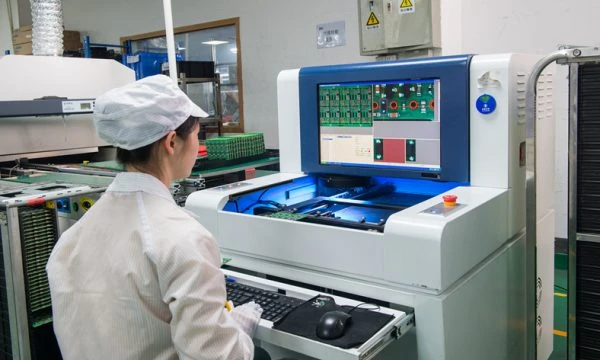
Automated Optical Inspection (AOI)
- Action: Scan the soldered board to check for visible defects like skew, tombstoning, or missing parts.
- Key Parameter: aoi vs x-ray inspection: what defects each catches (AOI catches line-of-sight issues).
- Acceptance: No flagged errors; false calls verified manually.
X-Ray Inspection (AXI)
- Action: Inspect hidden solder joints under BGAs, QFNs, and LGAs.
- Key Parameter: bga voiding control: stencil, reflow, and x-ray criteria (Voiding percentage).
- Acceptance: Voids < 25%; consistent ball shape and alignment.
Manual Visual Inspection
- Action: Human inspector checks for cosmetic issues, label placement, and non-standard components.
- Key Parameter: IPC-A-610 workmanship standards.
- Acceptance: No scratches, burns, or debris.
Impedance & Electrical Safety Check
- Action: Measure resistance between VCC and GND rails before applying power.
- Key Parameter: Resistance > 100Ω (or expected design value).
- Acceptance: No dead shorts on power lines.
Functional Testing (FCT)
- Action: Power up the board and run test firmware to validate logic and I/O.
- Key Parameter: Voltage levels (e.g., 3.3V ± 5%).
- Acceptance: Pass all functional test cases.
FAI Report Generation
- Action: Compile all data, images, and measurements into a signed document.
- Key Parameter: Traceability (Serial number, Date, Inspector).
- Acceptance: Signed approval from Quality Engineer.
Failure modes & troubleshooting
Even with a rigorous checklist, the first article may fail. Identifying the root cause quickly allows production to resume.
1. Tombstoning (Component standing on one end)
- Causes: Uneven heating, unbalanced pad sizes, or stencil aperture issues.
- Checks: Verify thermal relief design on pads; check if one pad is connected to a large ground plane without relief.
- Fix: Adjust reflow profile (soak zone) or modify stencil to reduce paste on the faster-melting pad.
- Prevention: Adhere to DFM guidelines regarding pad symmetry.
2. BGA Head-in-Pillow (HiP)
- Causes: Warped PCB or component, insufficient flux activity, or paste oxidation.
- Checks: Inspect component coplanarity and reflow profile peak temperature.
- Fix: Switch to a high-activity solder paste or use a nitrogen reflow environment.
- Prevention: Use lower-warpage PCB materials like Isola PCB for high-temp applications.
3. Solder Bridging (Shorts)
- Causes: Excessive solder paste, stencil apertures too large, or component placement pressure too high.
- Checks: Review SPI data for paste volume; check pick-and-place Z-height settings.
- Fix: Reduce stencil aperture size by 10% or clean the bottom of the stencil.
- Prevention: Implement frequent stencil cleaning cycles.
4. Cold Solder Joints
- Causes: Insufficient heat during reflow or disturbed joint during cooling.
- Checks: Analyze the reflow profile against the solder paste datasheet.
- Fix: Increase peak temperature or time above liquidus (TAL).
- Prevention: Regular oven profiling and thermocouple checks.
5. Misaligned Components
- Causes: Pick-and-place vision error, board fiducial recognition failure, or conveyor vibration.
- Checks: Verify fiducial clarity and machine vision coordinates.
- Fix: Recalibrate machine vision or clean fiducial markers on the PCB.
- Prevention: Ensure clear fiducials are included in the PCB manufacturing data.
6. De-wetting
- Causes: Contaminated pads, oxidized leads, or expired solder paste.
- Checks: Inspect PCB surface finish shelf life and paste expiration date.
- Fix: Bake PCBs to remove moisture or switch to fresh paste.
- Prevention: Proper storage of PCBs and moisture-sensitive devices (MSD).
Design decisions
The success of a first article inspection (fai) for pcba: checklist often depends on decisions made during the design phase.
- Test Points: Including accessible test points for all power rails and critical signals allows engineers to verify voltages easily during FAI without probing tiny component pins.
- Component Indicators: Clear silkscreen markings for polarity (e.g., a distinct dot for Pin 1 or a bar for cathodes) reduce manual inspection errors.
- Fiducials: Placing global and local fiducials ensures the pick-and-place machine aligns components accurately, reducing skew defects.
- Keep-out Zones: Adequate spacing around large components allows for rework tools and inspection equipment (like 45° AOI cameras) to function correctly.
- Material Selection: Choosing the right substrate, such as Rogers material for RF boards, ensures the board withstands reflow temperatures without warping, which is critical for BGA flatness.
FAQ
What is the main purpose of FAI in PCBA? FAI validates that the manufacturing process can consistently produce boards that meet design specifications. It acts as a gatekeeper before mass production to prevent volume scrap.
Is X-ray inspection mandatory for FAI? Yes, if the board contains BGAs, QFNs, or other bottom-terminated components. AOI vs x-ray inspection: what defects each catches differs; AOI cannot see beneath these parts to verify solder joint quality.
How does FAI differ from FAT (Factory Acceptance Testing)? FAI focuses on the manufacturing process and physical quality of the first unit. FAT is a broader test of the finished system's functionality, often done at the end of production.
What happens if the First Article fails? Production is halted. The root cause is identified (e.g., wrong stencil, bad part), corrected, and a new First Article is produced and inspected.
Does APTPCB perform FAI for all orders? APTPCB performs FAI for all new orders and major revisions. For repeat orders with no changes, standard process controls are used.
How long does the FAI process take? It typically adds 12 to 24 hours to the lead time of the first batch. This time is invested to ensure the thousands of boards that follow are correct.
Can I use a "Golden Board" for FAI? Yes, a known good board (Golden Board) is often used as a reference for AOI machines to compare against the new production units.
What is the acceptance standard for FAI? Most commercial electronics use IPC-A-610 Class 2. Medical, aerospace, and automotive applications typically require Class 3, which has tighter tolerances.
Does FAI check the bare PCB? The PCBA FAI assumes the bare PCB is good, but it does verify that the correct PCB revision was used. The bare PCB undergoes its own electrical test at the fab house.
Why is BGA voiding critical in FAI? BGA voiding control: stencil, reflow, and x-ray criteria are vital because voids reduce the thermal and mechanical performance of the joint. High voiding in the first article indicates a process drift that must be fixed.
Do I need to pay extra for FAI? At many contract manufacturers, FAI is included in the NRE (Non-Recurring Engineering) or setup costs. It is a standard part of quality assurance.
Can FAI be automated? Parts of it can (AOI, SPI, AXI), but the final sign-off usually requires a human quality engineer to review the data and physically handle the board.
What is a "Delta FAI"? A partial FAI performed when only a small change is made (e.g., replacing one capacitor value). Only the affected area is inspected.
Related pages & tools
- First Article Inspection (FAI): Understand what’s included in an assembly FAI and what data you’ll receive.
- PCB Manufacturing Services: Explore our capabilities for rigid, flex, and rigid-flex boards.
- Get a Quote: Start your project with a manufacturer that prioritizes rigorous FAI processes.
Glossary (key terms)
| Term | Definition |
|---|---|
| FAI | First Article Inspection; validation of the first production unit. |
| AOI | Automated Optical Inspection; camera-based check for visible defects. |
| AXI | Automated X-ray Inspection; uses X-rays to see hidden solder joints. |
| BOM | Bill of Materials; the list of all components required for the assembly. |
| SPI | Solder Paste Inspection; 3D measurement of paste deposits before placement. |
| IPC-A-610 | The industry standard for acceptability of electronic assemblies. |
| Reflow Profile | The temperature vs. time curve the PCB experiences in the oven. |
| Golden Board | A verified defect-free board used to calibrate inspection machines. |
| Tombstoning | A defect where a component stands up on one end during reflow. |
| Fiducial | A copper marker on the PCB used by machines for optical alignment. |
| MPN | Manufacturer Part Number; the specific ID for a component. |
| NPI | New Product Introduction; the phase where FAI is most critical. |
Conclusion
A disciplined first article inspection (fai) for pcba: checklist is the difference between a successful product launch and a costly recall. By verifying the BOM, validating solder joints via X-ray and AOI, and conducting electrical safety checks on the first unit, engineers ensure the integrity of the entire production run.
APTPCB integrates these rigorous checks into every NPI workflow, ensuring your design specifications are met with precision. Whether you are prototyping or scaling to volume, a verified first article provides the confidence needed to proceed.
For professional assembly with strict quality controls, submit your design to APTPCB today.