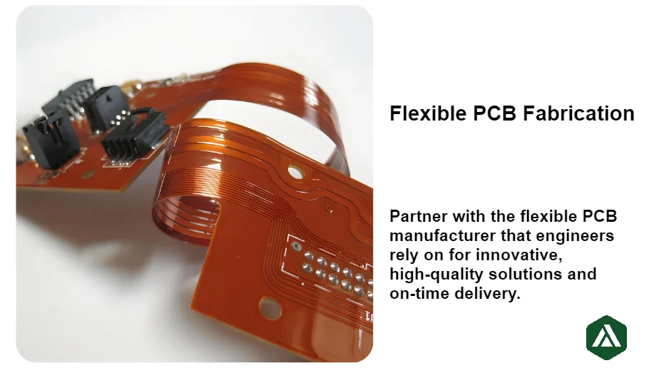
As electronics move toward thinner enclosures, tighter 3D packaging, foldable mechanisms, and wearable form factors, flexible PCBs (FPCs) have shifted from a “nice-to-have interconnect” to a core enabling technology. However, flexible PCB fabrication is not simply rigid PCB fabrication on a thin substrate. It is a coupled mechanical–electrical–process engineering problem where material system choices (PI/PET/LCP, RA/ED copper, adhesiveless vs adhesive-based), structural decisions (neutral axis placement, bend zone rules, stiffeners), and factory controls (laser drilling, plating integrity, coverlay registration, profiling) directly determine field reliability.
At APTPCB, we support global OEMs with China flexible PCB fabrication from design-for-manufacturability (DFM) through scalable production. If you need a quick capability reference, see our flex PCB and rigid-flex PCB offerings.
Menu Navigation
- 1) When a PCB Becomes “Flex”: Use Cases and Engineering Requirements
- 2) Material System Selection: PI vs PET vs LCP, Adhesiveless vs Adhesive-Based
- 3) Bend Reliability Engineering: Neutral Axis, Strain, and Bend Radius Rules
- 4) Flexible PCB Manufacturing Process: Laser Drilling, Plating, Coverlay, Finish, Profiling
- 5) Electrical Performance on Flex: Impedance Control, EMI, and Assembly Window
- 6) Quality Evidence and Reliability Testing: What to Specify and What to Verify
- 7) Cost Drivers and DFM Checklist: How to Reduce Flex PCB Cost Without Losing Reliability
1) When a PCB Becomes “Flex”: Use Cases and Engineering Requirements
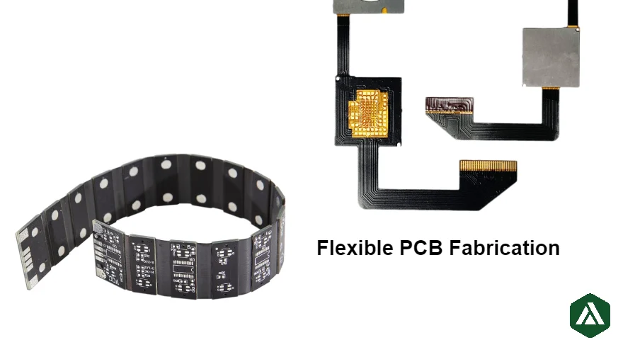
A flexible printed circuit (FPC) uses a bendable dielectric film (commonly polyimide) to route signals and power through compact or moving structures. The best reason to choose flex is not “it bends,” but that it replaces harnesses and connectors while enabling 3D packaging.
Typical use cases for flexible PCB fabrication
- Space-constrained consumer electronics: camera modules, displays, batteries, foldable subassemblies
- Wearables and medical devices: thin interconnects, micro-form-factor routing, movement tolerance
- Automotive electronics: sensors, lighting, battery management, vibration-prone systems
- Industrial automation and robotics: moving joints and repeat-motion interconnects
- Aerospace and defense: weight reduction and high-reliability routing in harsh environments
Translate “flex requirement” into measurable specifications
Before quoting or releasing design data, define flex requirements in engineering terms:
- Bend type: static bend (formed once) vs dynamic bend (repeated cycling)
- Bend profile: minimum bend radius, bend angle, bend length, and cycle count
- Mechanical constraints: hinge geometry, insertion paths, keep-out zones, stiffener needs
- Assembly exposure: number of reflow cycles, peak temperature limits, selective solder constraints
- Environment: temperature range, humidity, chemicals, vibration/shock requirements
These details directly drive copper selection (RA vs ED), stack-up choice (adhesiveless vs adhesive-based), and coverlay strategy.
2) Material System Selection: Polyimide (PI) vs Polyester (PET) vs Liquid Crystal Polymer (LCP), Adhesiveless vs Adhesive-Based
In flexible PCB fabrication, material selection is the highest-leverage decision. Choosing the wrong system often creates fatigue cracks, registration instability, delamination, and impedance drift—problems that are expensive to “patch” later.
Substrate selection: PI vs PET vs LCP
Polyimide (PI) The most common engineering-grade flex substrate. PI supports high reflow temperatures, maintains stable electrical properties, and provides a balanced mechanical profile for most applications—including many dynamic flex designs.
Polyester (PET) A lower-cost alternative suited to static flex applications with lower temperature requirements. PET is usually not recommended for repeated bending or high-temperature assembly where dimensional stability and heat resistance matter.
Liquid Crystal Polymer (LCP) A premium substrate for advanced RF/high-frequency or moisture-sensitive applications. LCP offers low dielectric loss and strong humidity stability—valuable for mmWave antennas and certain medical/RF modules. Processing windows are tighter, and cost is higher.
Adhesiveless vs adhesive-based flex stack-ups
Adhesiveless (adhesive-free) flex
- Better high-temperature stability and often improved dynamic bend reliability
- Less risk of adhesive flow during reflow
- Typically preferred for high-reliability products and repeated bending zones Common search intent: “adhesiveless flexible PCB manufacturer”, “adhesive-free flex PCB for dynamic bending”.
Adhesive-based flex
- More cost-effective and widely used for static flex
- Requires tighter control of adhesive flow, voids, and interface behavior under reflow and thermal cycling Common search intent: “adhesive-based flex PCB limitations”, “coverlay adhesive flow in reflow”.
Copper selection: RA copper vs ED copper
This is one of the most searched and most misunderstood topics in flex PCB fabrication.
RA copper (Rolled Annealed copper)
- Higher ductility and better fatigue resistance
- Recommended for dynamic flex PCB designs (repeated bending cycles)
- Better suited for hinge zones and motion assemblies
ED copper (Electro-Deposited copper)
- Lower cost, widely used in static flex applications
- Can fatigue sooner in high-cycle bending scenarios
If your product spec includes “bend cycles,” RA copper is usually the default starting point.
Coverlay vs LPI solder mask
Coverlay The standard protective dielectric layer for flex. It performs well in bend zones due to flexibility and mechanical durability.
LPI solder mask Often used selectively in high-density soldering regions for finer feature control (mask dams, tight openings). It is generally less bend-friendly than coverlay, so many designs use coverlay for bend zones and LPI only where assembly density demands it.
3) Bend Reliability Engineering: Neutral Axis, Strain, and Bend Radius Rules
Flex reliability is not about “can it bend,” but “how long until it fails.” The engineering center is strain management, strongly influenced by the neutral axis location and the copper’s distance from it.
Why neutral axis matters
In bending, outer layers experience tensile strain and inner layers compressive strain. The neutral axis is the region where strain is near zero. Copper placed farther from the neutral axis sees higher strain and faster fatigue. Practical implication: stack-up design is bend-life design.
Static vs dynamic bend rules (design intent must be explicit)
Static bend (formed once or rarely)
- Smaller bend radii may be acceptable
- Still avoid sharp folds, hard transitions, and stress concentrators near pads/vias/stiffener edges
Dynamic bend (repeated cycling)
- Use larger radii, RA copper, and simplified bend-zone structures
- Avoid vias, pads, test points, and stiffener edges in the active bend region
- Use smooth geometry and stress-relief features
Bend zone layout rules that improve lifetime
- Route traces perpendicular to the bend axis where possible
- Avoid 90° corners; use arcs or gentle angles
- Use teardrops at pad/via transitions to reduce stress concentration
- Avoid copper “rigidity jumps”: abrupt copper pours or thick local copper in bend zones
- Keep bend zones free of plated through holes and rigid constraints
- Separate bend zones from stiffener edges and connector insert areas
Designing for fatigue: what to specify on drawings
A professional flex drawing package typically calls out:
- Bend region boundaries (bend line and keep-out)
- Minimum bend radius and target cycles
- Static vs dynamic classification
- Copper type requirement (RA in dynamic zones)
- Restrictions: no vias/components in active bend area
- Any special test requirement (bend life validation, resistance monitoring)
4) Flexible PCB Manufacturing Process: Laser Drilling, Plating, Coverlay, Finish, Profiling
A capable China flexible PCB manufacturer should control four “make-or-break” variables: registration, plating integrity, coverlay alignment, and outline quality.
Step 1: Material prep and dimensional control
Flex materials are more sensitive to humidity and handling. Proper storage, pre-bake strategies (where required), and process compensation reduce registration drift and warpage.
Step 2: Drilling and laser microvias
- Mechanical drilling for larger holes and cost control
- Laser drilling for microvias, HDI interconnects, and fine structures Engineering alignment of hole size, density, and tolerance is critical; manufacturing controls are commonly defined under PCB drilling capability constraints.
Step 3: Imaging and etching (fine-line stability)
Fine line/space stability depends on photo process control, etch factor management, and copper thickness uniformity. Flex designs often require tighter process discipline because thin dielectrics amplify impedance and spacing sensitivity.
Step 4: PTH plating integrity (reliability hotspot)
In flex circuits—especially in rigid-flex transitions—plated through holes can become failure points under thermal cycling and mechanical stress. The manufacturing focus is:
- Consistent copper thickness in barrels
- Clean hole walls and strong interface adhesion
- Controlled thermal excursions to reduce microcracking risk
Step 5: Coverlay lamination and openings
Coverlay is essential but introduces yield risk when openings are dense or tolerances are tight:
- Opening registration and alignment to pads
- Edge quality of openings (stress and peel risk)
- Adhesive flow control to prevent pad contamination
Step 6: Surface finish selection
Finish choice affects solderability, flatness, storage life, and assembly yield. Many flex programs choose ENIG for fine pitch; OSP can be cost-effective but more storage-sensitive; immersion tin can be used when flatness is critical. For selection guidance, see PCB surface finishes.
Step 7: Stiffeners (connector and SMT support zones)
Stiffeners are structural components, not “optional add-ons.” Key controls:
- Material choice (FR-4, PI, stainless steel)
- Thickness and flatness targets for connector fit
- Adhesive selection and alignment tolerance
- Smooth edge transitions to avoid stress concentration
Step 8: Profiling and outline processing
- Punching for high-volume and low per-unit cost (tooling required)
- Laser cutting for prototypes and complex shapes (no tooling, slower cycle)
- CNC routing for mid-volume flexibility and edge-quality control Outline control is typically managed via PCB profiling requirements.
Step 9: Electrical test and final inspection
- 100% open/short testing (fixture or flying probe depending on design)
- Visual inspection focused on coverlay alignment, copper defects, contamination, and edge quality
- Optional hi-pot testing for insulation strength
5) Electrical Performance on Flex: Impedance Control, Electromagnetic Interference (EMI), and Assembly Window
Flex “thinness” makes impedance control both easier and riskier: easier because geometry can produce certain impedances at small widths; riskier because small variations in thickness, coverlay, and copper can shift impedance noticeably.
Controlled impedance on flex
Professional impedance planning includes:
- Defining microstrip/stripline/coplanar structures intentionally
- Accounting for coverlay and adhesive layers in effective dielectric thickness
- Avoiding abrupt geometry changes at pads and transitions
- Using test coupons and acceptance tolerance for verification
EMI and return path continuity
Flex circuits often route through mechanical openings and folds—exactly where return paths can be compromised.
- Keep high-speed nets referenced to continuous ground where possible
- Avoid routing across plane gaps or large reference changes
- Plan return path transitions deliberately when changing layers or crossing splits
- In dynamic zones, evaluate mesh ground tradeoffs: mechanical benefit vs return-current performance
Assembly window: reflow sensitivity and solder joint reliability
Flex assemblies may experience:
- Adhesive flow risks during reflow
- Local thermal mass differences near stiffeners and connectors
- Warpage affecting fine-pitch yields
Successful programs align coverlay opening tolerances, surface finish selection, and reflow profiles early—before NPI builds.
6) Quality Evidence and Reliability Testing: What to Specify and What to Verify
For flex PCBs, “passed electrical test” is not enough. You need evidence that the design survives mechanical and thermal stress.
What a serious supplier should provide (process + product evidence)
- Incoming material controls (substrate thickness, copper type, adhesive system verification)
- Registration and dimensional reports where critical
- Electrical test records (100% continuity/isolation)
- Targeted cross-sections for plating integrity and interface quality (sampling plan)
- Final inspection criteria and acceptance standards
Quality frameworks are often summarized under PCB quality expectations.
Reliability tests commonly specified for flexible PCB fabrication
- Dynamic bend life test (cycles, angle, radius, resistance monitoring)
- Peel strength test (copper/laminate and coverlay adhesion)
- Thermal cycling (plating integrity, interface stability)
- Solderability / multiple reflow simulation (finish and coverlay/adhesive behavior)
- Humidity or chemical exposure (depending on end-use environment)
7) Cost Drivers and global OEMs with China flexible PCB fabrication from design-for-manufacturability (DFM) Checklist: How to Reduce Flex PCB Cost Without Losing Reliability
Many buyers search “low cost flex PCB,” but cost is controlled by yield and processing time, not only raw material price.
Major cost drivers in China flexible PCB fabrication
- Layer count and total thickness
- Fine line/space and tight registration tolerances
- Laser microvia density and drilling time
- Complex coverlay openings and tight opening-to-pad tolerances
- Stiffener quantity, materials, and alignment requirements
- Complex outline shapes and whether punching tooling is required
- Surface finish choice (ENIG vs OSP vs immersion tin)
- Reliability testing scope and documentation requirements
DFM checklist (practical, quote-ready)
- Specify static vs dynamic bend intent and cycle requirements
- Define bend zones clearly (keep-outs, bend line, bend radius, cycle count)
- Require RA copper in dynamic zones; avoid vias/components in active bend regions
- Confirm coverlay strategy and opening tolerances early
- Provide stiffener drawings (material, thickness, location, tolerance, adhesive spec)
- Choose profiling method appropriate to volume (laser prototype → punch volume)
- Specify surface finish and storage/assembly expectations
- Confirm inspection and reliability evidence requirements (bend test, thermal cycle, cross-section)
If you need rapid iteration, you can align early programs with quick turn PCB workflows, then transition to production controls for scaling.
FAQ
What is the best material for flexible PCB fabrication—PI vs PET vs LCP?
For most high-reliability products, polyimide (PI) is the default. PET is often used for low-cost static flex with lower temperature requirements. LCP is typically selected for high-frequency/RF or moisture-sensitive applications where low loss and dimensional stability are critical.
RA copper vs ED copper—what’s the difference for dynamic flex PCB design?
RA copper provides better ductility and fatigue life for repeated bending, making it the preferred choice for dynamic flex PCB designs. ED copper is cost-effective for static flex but can fatigue earlier in high-cycle bending zones.
What does “adhesiveless flexible PCB” mean and when should I choose it?
An adhesiveless flex PCB uses an adhesive-free copper-to-polyimide structure that generally improves high-temperature stability and can enhance bend reliability. It is commonly chosen for dynamic flex, high-reflow exposure, and high-reliability programs.
Coverlay vs solder mask on flex PCB—what should I use?
Coverlay is the standard for bend zones and mechanical protection in FPCs. LPI solder mask can be used where fine solder mask definition is needed for dense SMT pads, often applied selectively rather than across the entire flex.
How do I calculate minimum bend radius for a flexible PCB?
Minimum bend radius depends on total thickness, layer count, copper type (RA vs ED), and whether the bend is static or dynamic. For dynamic bending, larger radii are typically required, and design rules should keep vias, pads, and stiffener edges out of the active bend zone.
Can I place vias in a flex PCB bend area?
It is strongly discouraged for dynamic bend zones. Vias are stress concentrators and frequent failure sites. If a via cannot be avoided, treat it as a high-risk region: increase bend radius, adjust stack-up to reduce strain, and validate with bend-life testing.
What surface finish is best for flexible PCB assembly (ENIG vs OSP vs immersion tin)?
ENIG is often selected for fine pitch due to flatness and oxidation resistance. OSP is cost-effective but more storage-sensitive. Immersion tin can be useful where flatness is critical. The best choice depends on assembly process, storage duration, and pad geometry.
What is the difference between rigid-flex PCB fabrication and flex PCB fabrication?
Rigid-flex PCB fabrication integrates rigid sections (for component mounting and stiffness) with flex interconnects in one structure, reducing connectors and improving reliability. Standard flex PCB fabrication is typically a flexible interconnect without rigid sections, often combined with connectors or stiffeners.
How do I choose a flex PCB manufacturer in China for high reliability?
Look for documented controls on materials (PI/LCP options, RA copper availability), laser drilling and plating capability, coverlay registration accuracy, electrical test coverage, reliability testing options (bend life, thermal cycling), and clear DFM feedback. Ask for cross-section evidence and process traceability on critical builds.
What files do I need to get an accurate quote for China flexible PCB fabrication?
Provide Gerber/ODB++, stack-up or material targets (PI/PET/LCP, adhesiveless/adhesive-based), copper type (RA/ED), coverlay strategy, stiffener drawings, outline/profile requirements, surface finish, bend zone definition (radius/cycles), quantity, and target lead time.
Conclusion
Professional China flexible PCB fabrication is a reliability discipline: you must match the material system to bend intent, design bend zones around neutral axis and strain management, control manufacturing variables like plating integrity and coverlay registration, and validate with the right mechanical and thermal evidence.
APTPCB supports engineering-driven flexible PCB projects from prototype to volume production—covering flex PCB and rigid-flex PCB—with process controls for drilling, surface finish selection, profiling, and quality assurance aligned to demanding applications.