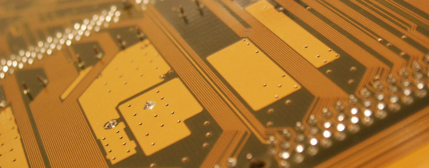
Successful flexible pcb fabrication requires a fundamental shift in mindset from rigid board design. Unlike FR4, flexible circuits (FPC) rely on Polyimide (PI) substrates that introduce unique challenges regarding dimensional stability, moisture absorption, and mechanical stress management. Engineers must account for material shrinkage during lamination and ensure the copper grain structure aligns with the bend direction to prevent fatigue failure.
At APTPCB (APTPCB PCB Factory), we see that the majority of flex circuit failures stem not from the manufacturing process itself, but from layout decisions that ignore the physical limitations of thin dielectrics. This guide provides the technical specifications, process steps, and validation protocols necessary to produce reliable flexible PCBs for dynamic and static applications.
flexible pcb fabrication quick answer (30 seconds)
- Material Selection is Critical: Use Rolled Annealed (RA) copper for dynamic flexing applications; Electro-Deposited (ED) copper is acceptable only for static (install-to-fit) designs.
- Bend Radius Rules: Adhere strictly to flex pcb bend radius rules. Maintain a minimum radius of 6x thickness for static bends and roughly 10x-20x for dynamic flexing to avoid work hardening and cracking.
- Coverlay vs. Solder Mask: Prefer Polyimide coverlay for flexibility and dielectric strength. Use flexible solder mask only for high-density component areas where coverlay web width is insufficient.
- Stiffener Strategy: Apply FR4 or Polyimide stiffeners under components and connectors to prevent solder joint fractures; the flex area must remain free of stiffeners.
- Dimensional Stability: Flexible materials shrink and stretch during processing. Design with loose tolerances (±0.05mm to ±0.10mm) compared to rigid boards.
- Tear Drops are Mandatory: Always add teardrops to pad-trace interfaces to reduce stress concentration and prevent cracks during thermal expansion or mechanical flexing.
When flexible pcb fabrication applies (and when it doesn’t)
Understanding the mechanical requirements of the final assembly dictates whether a pure flex or rigid-flex solution is required.
When to use flexible pcb fabrication:
- Dynamic Motion: The device requires continuous movement, such as print heads, disk drives, or wearable hinges.
- 3D Packaging: The circuit must fold into complex shapes to fit inside compact housings (cameras, hearing aids).
- Weight Reduction: Aerospace or drone applications where eliminating heavy wire harnesses and connectors is a priority.
- Vibration Resistance: The low mass and ductility of flex circuits make them more reliable than rigid boards in high-vibration environments.
- High-Density Interconnects: Replacing bulky ribbon cables with fine-pitch etched traces.
When NOT to use it:
- Load Bearing: Flex PCBs cannot support heavy components (transformers, large capacitors) without extensive stiffening, which negates the cost benefit.
- High-Current Power Distribution: While heavy copper flex exists, thermal management is difficult due to the thin dielectric; rigid boards or busbars are often better.
- Ultra-Low Cost Consumer Goods: If a simple wire harness or a standard FR4 board fits, flex fabrication is typically 2-3x more expensive due to material and handling costs.
- Large Flat Surfaces: Using flex material for a large, flat motherboard is inefficient; use rigid PCBs for the main logic and flex only for interconnects.
flexible pcb fabrication rules and specifications (key parameters and limits)
The following parameters define the boundaries of manufacturable flexible pcb fabrication. Ignoring these often leads to yield loss or field failure.
| Rule | Recommended Value/Range | Why it matters | How to verify | If ignored |
|---|---|---|---|---|
| Min Trace/Space | 3mil / 3mil (0.075mm) | Flex materials are harder to etch precisely due to dimensional instability. | AOI (Automated Optical Inspection). | Shorts, opens, or impedance mismatches. |
| Annular Ring | Min 4mil (0.10mm) larger than hole | Material movement during lamination causes misregistration. | CAM review of pad vs. drill size. | Breakout (drill hitting edge of pad), open circuits. |
| Bend Radius (Dynamic) | > 10x - 20x Board Thickness | Prevents copper fatigue and work hardening during repeated motion. | CAD simulation or physical bend test. | Conductor cracking after limited cycles. |
| Bend Radius (Static) | > 6x Board Thickness | Prevents immediate fracture during installation folding. | CAD mechanical constraints. | Copper fracture during assembly installation. |
| Coverlay Web | Min 6mil (0.15mm) | Narrow strips of coverlay adhesive do not bond well and may lift. | DFM check of coverlay openings. | Coverlay delamination or adhesive flow onto pads. |
| Stiffener Overlap | Overlap coverlay by 10-20mil | Prevents a stress concentration point (weak spot) at the stiffener edge. | Stackup drawing review. | Trace fracture exactly at the stiffener edge. |
| Pad Plating | ENIG or Soft Gold | Hard gold is brittle and cracks; HASL is too uneven for flex. | X-Ray Fluorescence (XRF). | Cracking of surface finish or poor solderability. |
| Teardrops | Required on all pads | Distributes mechanical stress at the junction of trace and pad. | Visual inspection of Gerber files. | Cracks at the pad-trace interface during thermal cycling. |
| Adhesive Flow | Keep 5-10mil away from pads | Adhesive squeezes out during lamination; can contaminate pads. | DFM clearance check. | Solderability failure (solder won't wet the pad). |
| Impedance Control | ±10% Tolerance | Dielectric thickness of PI varies; hatching ground planes helps. | TDR (Time Domain Reflectometry). | Signal integrity issues in high-speed data lines. |
| Copper Type | RA (Rolled Annealed) | RA copper has a horizontal grain structure allowing flexibility. | Material certification (IPC-4562). | Immediate cracking upon flexing if ED copper is used dynamically. |
| Via Placement | Keep away from bend areas | Plated barrels are rigid and will crack if bent. | Design Rule Check (DRC). | Intermittent open circuits during operation. |
flexible pcb fabrication implementation steps (process checkpoints)
Executing flexible pcb fabrication involves distinct steps that differ from rigid board processing.
Material Preparation & Stabilization:
- Action: Cut Polyimide (PI) and copper clad laminates (CCL) to panel size. Bake the material for 2-4 hours.
- Key Parameter: Temperature (typically 120°C-150°C) to remove moisture.
- Acceptance Check: No blistering or deformation; dimensional measurement baseline established.
Circuit Patterning (Inner/Outer Layers):
- Action: Apply photoresist, expose, develop, and etch the copper traces.
- Key Parameter: Etch compensation factors must be higher than rigid boards due to flexible material movement.
- Acceptance Check: Trace width within ±15% tolerance; no residual copper shorts.
Automated Optical Inspection (AOI):
- Action: Scan etched layers for opens, shorts, and neck-downs.
- Key Parameter: Resolution set to detect defects down to 0.5mil.
- Acceptance Check: Pass/Fail report; zero open/short defects allowed.
Coverlay Lamination:
- Action: Align pre-drilled or laser-cut coverlay film over the etched circuits. Tack in place and press.
- Key Parameter: Lamination pressure (200-300 PSI) and temperature profile.
- Acceptance Check: No air bubbles, no adhesive flow onto solder pads, proper registration.
Drilling & Plating (Through-Hole):
- Action: Mechanical or laser drilling of vias, followed by desmear and copper plating.
- Key Parameter: Desmear plasma treatment is crucial to remove acrylic/epoxy adhesive smear from hole walls.
- Acceptance Check: Hole wall quality (smoothness) and plating thickness (min 20µm average).
Surface Finish Application:
- Action: Apply ENIG (Electroless Nickel Immersion Gold) or Immersion Silver.
- Key Parameter: Nickel thickness (3-6µm) to prevent oxidation without making the pad brittle.
- Acceptance Check: Solderability test and thickness verification via XRF.
Stiffener Application:
- Action: Bond FR4, PI, or Stainless Steel stiffeners to specific areas using pressure-sensitive adhesive (PSA) or thermoset adhesive.
- Key Parameter: Alignment accuracy (±0.1mm) and adhesive curing cycle.
- Acceptance Check: Stiffener adhesion strength; no voids in adhesive layer.
Electrical Testing & Profiling:
- Action: Flying probe test for continuity/isolation, followed by laser cutting or die punching to final shape.
- Key Parameter: Isolation resistance (>10MΩ) and outline tolerance (±0.05mm).
- Acceptance Check: 100% Netlist match; clean edges with no burrs.
flexible pcb fabrication troubleshooting (failure modes and fixes)
Failures in flexible pcb fabrication are often mechanical or material-related.
1. Conductor Cracking in Bend Area
- Symptom: Intermittent open circuits when the device is moved or folded.
- Causes: Bend radius too tight; wrong copper type (ED instead of RA); traces running perpendicular to bend axis; stacked traces (I-beam effect).
- Checks: Microsection analysis of the crack; review grain direction.
- Fix: Increase bend radius; switch to RA copper; stagger traces on different layers.
- Prevention: Follow flex pcb bend radius rules strictly during layout.
2. Coverlay Delamination
- Symptom: Bubbles or separation between the coverlay and base copper/PI.
- Causes: Trapped moisture before lamination; insufficient lamination pressure; contaminated surface.
- Checks: Bake test; inspect for foreign material.
- Fix: Optimize pre-bake cycle (remove moisture); adjust press profile.
- Prevention: Store materials in humidity-controlled cabinets; ensure thorough cleaning before lamination.
3. Solder Joint Fracture (at Stiffener Edge)
- Symptom: Components near the stiffener edge pop off or show cracked solder joints.
- Causes: Stress concentration where the flexible part meets the rigid stiffener.
- Checks: Visual inspection of the transition zone.
- Fix: Extend the stiffener slightly under the coverlay (overlap) or move components further away (min 3mm) from the stiffener edge.
- Prevention: Design stiffeners to overlap the coverlay by 10-20 mils to create a gradual stress transition.
4. Pad Lifting
- Symptom: Copper pads peel off the PI substrate during soldering.
- Causes: Excessive heat; no adhesive anchoring; lack of "toe-down" design.
- Checks: Peel strength test.
- Fix: Use "anchor spurs" or larger annular rings; reduce soldering temperature/time.
- Prevention: Use adhesiveless laminates for higher thermal resistance; add mechanical anchors to pads.
5. Barrel Cracks (Plated Through Holes)
- Symptom: Open vias after thermal cycling or soldering.
- Causes: Z-axis expansion of the acrylic adhesive is high; poor plating ductility.
- Checks: Thermal shock test; cross-sectioning.
- Fix: Use adhesiveless base materials (eliminates acrylic adhesive); increase copper plating thickness.
- Prevention: Minimize vias in flex areas; use teardrops on all via connections.
6. Solder Wicking under Coverlay
- Symptom: Solder flows under the coverlay, causing shorts or stiffening the flex area.
- Causes: Coverlay opening too large; adhesive dam insufficient.
- Checks: Visual inspection after wave/reflow.
- Fix: Reduce coverlay opening size; use solder mask dams if geometry allows.
- Prevention: Define coverlay openings 1:1 with pads or slightly smaller (solder mask defined) if pitch allows.
How to choose flexible pcb fabrication (design decisions and trade-offs)
Making the right choices early in the design phase prevents costly revisions.
Coverlay vs Solder Mask on Flex PCB
This is a common point of confusion.
- Coverlay (Polyimide + Adhesive): The standard for flex. It is a solid sheet laminated onto the board. It offers superior flexibility and dielectric strength. However, it requires drilling or laser cutting, limiting the minimum opening size and shape (usually square or circular). Fine pitch components are difficult to define with coverlay.
- Flexible Solder Mask (Liquid Photoimageable): Applied like paint. It allows for very fine resolution (tight dams between pads) similar to rigid boards. However, it is brittle compared to coverlay. Decision Rule: Use coverlay for the flexible "arms" and dynamic areas. Use flexible solder mask only on rigidized areas where fine-pitch components (BGA, QFN) are mounted.
Material Stackup: Adhesive vs. Adhesiveless
- Adhesive-based (3-layer): Copper + Acrylic Adhesive + Polyimide. Cheaper, higher peel strength, but the adhesive has a high Z-axis expansion (bad for vias) and lower temperature rating.
- Adhesiveless (2-layer): Copper sputtered or cast directly on Polyimide. Thinner, better for controlled impedance, better thermal performance, and more reliable vias. APTPCB recommends adhesiveless for high-reliability or high-frequency designs.
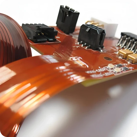
Stiffener Types
- FR4: Used to rigidize areas for component assembly. Same material as rigid PCBs.
- Polyimide: Used to add thickness to ZIF (Zero Insertion Force) connector fingers (typically 0.3mm total thickness required).
- Stainless Steel/Aluminum: Used for heat sinking or providing a very rigid backing for keypads.
flexible pcb fabrication FAQ (cost, lead time, Design for Manufacturability (DFM) files, stackup, impedance, Automated Optical Inspection (AOI) inspection)
1. What is the standard thickness for a flexible PCB? The most common total thickness is 0.10mm to 0.15mm for a 2-layer flex. However, this varies based on copper weight (0.5oz or 1oz) and PI thickness (1mil or 2mil).
2. Can I use standard FR4 design rules for flex? No. Flex requires larger annular rings, teardrops on all pads, and wider trace-to-edge clearances. Standard rigid rules will lead to manufacturing yield loss.
3. Why is "hatching" used on ground planes? Solid copper planes reduce flexibility and can cause the board to buckle. Cross-hatched copper retains electrical continuity while significantly improving flexibility.
4. What is the difference between static and dynamic flex? Static flex (flex-to-install) is bent once during assembly and stays fixed. Dynamic flex bends repeatedly during operation. Dynamic designs require RA copper and stricter bend radius controls.
5. How do I specify stiffeners in my Gerber files? Create a separate mechanical layer in your Gerber data outlining the stiffener shape and indicating the material (e.g., "FR4 Stiffener, 0.8mm thick, Top Side").
6. Can I put vias in the bend area? Avoid this whenever possible. Plated holes are rigid stress points that will crack under stress. If unavoidable in static flex, place them in areas with minimal stress.
7. What is the cost difference between flex and rigid PCBs? Flex PCBs are typically 2-5 times more expensive per square inch than rigid boards due to material costs, manual handling (lamination, stiffener application), and lower panel utilization.
8. How does impedance control work on flex? Impedance is controlled by trace width, spacing, and dielectric thickness. Since PI dielectrics are thin, traces must often be narrower. Adhesiveless materials provide better consistency for high-speed signals.
9. What is a "Bikini Cut" coverlay? This refers to a design where coverlay is applied only to the flexible sections, while the rigid/component areas use solder mask. This combines the flexibility of coverlay with the fine pitch capability of solder mask.
10. Why do I need to bake flex PCBs before soldering? Polyimide is hygroscopic (absorbs moisture). If not baked (e.g., 120°C for 2-4 hours) before reflow, the trapped moisture turns to steam and causes delamination (popcorning).
11. What is the minimum bend radius I should use? For single-sided: 3-6x thickness. For double-sided: 6-10x thickness. For multilayer: 10-20x thickness. Always calculate based on the total thickness of the flex section.
12. Can APTPCB manufacture rigid-flex boards? Yes, we specialize in complex rigid-flex PCB integration, combining the stability of FR4 with the versatility of flex layers in a single unit.
Resources for flexible pcb fabrication (related pages and tools)
- Flex PCB Capabilities: Detailed specs on layer counts, materials, and tolerances.
- DFM Guidelines: Essential design rules to ensure your board is manufacturable.
- PCB Stack-up Planning: How to structure layers for impedance and flexibility.
flexible pcb fabrication glossary (key terms)
| Term | Definition |
|---|---|
| Polyimide (PI) | The primary dielectric material used in flex circuits; known for high heat resistance and flexibility. |
| Coverlay | A laminate of PI and adhesive used to insulate outer layers; replaces solder mask in flex areas. |
| Stiffener | A rigid piece of material (FR4, PI, Metal) bonded to the flex to support components or connectors. |
| RA Copper | Rolled Annealed Copper. The grain structure is horizontal, making it highly ductile and suitable for dynamic flexing. |
| ED Copper | Electro-Deposited Copper. The grain structure is vertical; brittle and suitable only for static applications. |
| Adhesiveless Laminate | Copper bonded directly to PI without acrylic adhesive; better for high-temp and high-frequency apps. |
| ZIF Connector | Zero Insertion Force connector. Requires tight tolerance on flex thickness and stiffener backing. |
| Bikini Cut | A method where coverlay covers the flex arm, but stops short of the component area, which is covered by solder mask. |
| PSA | Pressure Sensitive Adhesive. Like double-sided tape, used to attach stiffeners (not for reflow soldering adhesion). |
| I-Beam Effect | Stiffness increase caused by stacking traces on top of each other on adjacent layers; increases risk of cracking. |
| Teardrop | A widening of the trace as it enters a pad; reduces stress concentration and prevents cracking. |
| Springback | The tendency of a flex circuit to return to its flat state after bending; must be accounted for in mechanical design. |
Request a quote for flexible pcb fabrication (Design for Manufacturability (DFM) review + pricing)
Ready to move to production?
- Request a Quote: Submit your design for a comprehensive DFM review and pricing.
- What to send:
- Gerber Files: RS-274X format preferred.
- Fab Drawing: Must specify stackup, materials (RA vs ED), coverlay type, and stiffener locations.
- Quantities: Prototype vs. Mass Production volumes affect tooling choices (laser vs. die cut).
- Special Requirements: Impedance control, specific bend radius needs, or PSA specifications.
Conclusion (next steps)
Flexible pcb fabrication is a specialized process that demands rigorous attention to material properties and mechanical stress. By selecting the right copper type, adhering to bend radius constraints, and designing robust stackups with appropriate stiffeners, engineers can deploy reliable flex circuits in the most demanding environments. APTPCB is equipped to guide you through these technical decisions, ensuring your design transitions smoothly from prototype to volume production.