Definition, scope, and who this guide is for
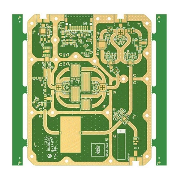
GaN power stage PCB impedance control refers to the precise management of trace dimensions, layer stackups, and dielectric materials to maintain signal integrity and minimize parasitic inductance in Gallium Nitride (GaN) circuits. Unlike silicon-based designs, GaN devices switch at extremely high speeds (high dv/dt and di/dt). Without strict impedance control, these fast switching edges cause voltage overshoot, ringing, and electromagnetic interference (EMI) that can destroy the device or fail regulatory testing.
This guide is written for Engineering Managers and Procurement Leads who are transitioning designs from standard silicon MOSFETs to GaN technology. It focuses on the manufacturing reality of these boards. You do not need to be a physicist to use this guide; you need to be a decision-maker looking to secure a reliable supply chain.
The scope covers the critical intersection of GaN power stage PCB design and fabrication. We address how to specify requirements that a factory can actually build, how to validate the results, and how to avoid common procurement pitfalls. APTPCB (APTPCB PCB Factory) developed this playbook to bridge the gap between theoretical simulation and physical production.
When to use this approach (and when not to)
Understanding the scope of GaN requirements helps determine if your project truly requires the cost premiums associated with advanced impedance control or if standard fabrication suffices.
Use strict GaN power stage PCB impedance control when:
- Switching Frequency exceeds 500 kHz: At these speeds, parasitic inductance in the gate loop becomes a critical failure point.
- High Power Density Designs: Applications like server power supplies or EV on-board chargers where components are tightly packed require HDI (High Density Interconnect) techniques with controlled impedance.
- Fast Rise Times (<10ns): If your GaN transistors are switching in nanoseconds, the PCB traces act as transmission lines, requiring matched impedance to prevent reflections.
- RF Power Amplifiers: GaN is standard in RF; here, impedance matching is non-negotiable for power transfer efficiency.
A standard approach is better when:
- Legacy Silicon Designs: If you are using standard Si-MOSFETs switching under 100 kHz, standard tolerances (+/- 10%) are usually sufficient.
- Low-Speed Aux Circuits: The control logic or housekeeping power rails on the same board may not need the same expensive materials as the main power stage.
- Prototyping for Fit/Form: If the goal is mechanical verification only, you can bypass expensive impedance testing to save time.
Specs to define (materials, stackup, tolerances)
Once you have determined that your project requires high-performance fabrication, you must define clear specifications to align your design team with the manufacturer.
- Dielectric Material Selection: Specify materials with stable Dielectric Constant (Dk) and low Loss Tangent (Df) across high frequencies. Common choices include high-Tg FR4 for lower frequencies or Rogers/Isola laminates for RF-class GaN applications.
- Layer Stackup Symmetry: Define a balanced stackup to prevent warpage. For GaN, the distance between the top layer (component) and the first inner reference plane (GND) must be minimized to reduce loop inductance.
- Impedance Tolerance: Move from the standard +/- 10% to +/- 5% or +/- 7% for critical gate drive and power loop traces.
- Copper Weight: Specify copper weight carefully. While heavy copper (2oz+) is good for thermal management, it makes fine-line etching for impedance control more difficult.
- Trace Width and Spacing: Define minimum trace width/spacing based on the copper weight. For 1oz copper, 4mil/4mil is standard; for 2oz, 6mil/6mil is safer.
- Via Types: Specify if blind or buried vias are required. GaN designs often use "via-in-pad" plated over (POFV) to minimize inductance paths directly under the component thermal pad.
- Surface Finish: ENIG (Electroless Nickel Immersion Gold) or ENEPIG is preferred over HASL. The flat surface of ENIG is critical for the precise placement of small GaN packages (e.g., CSP or QFN).
- Solder Mask: Specify LPI (Liquid Photoimageable) solder mask. Note that solder mask thickness affects impedance; the manufacturer must account for this in their calculations.
- Peel Strength: GaN devices run hot. Ensure the laminate has high copper peel strength to prevent delamination under thermal cycling.
- Glass Weave Style: Request "spread glass" or tighter weave styles (e.g., 1067, 1080) to minimize the "fiber weave effect" which can cause skew in high-speed differential pairs.
- Cleanliness Requirements: Ionic contamination must be strictly controlled to prevent dendritic growth under high voltage fields.
- Documentation: Require an impedance control report included with the shipment, verifying TDR measurements against the design files.
Manufacturing risks (root causes & prevention)
Even with perfect specifications, the physical manufacturing process introduces variables that can disrupt GaN power stage PCB impedance control; identifying these risks early prevents scrap.
Risk: Etch Factor Variation
- Root Cause: As copper gets thicker, the chemical etchant removes copper from the top of the trace faster than the bottom, creating a trapezoidal shape.
- Detection: Cross-section analysis (microsection).
- Prevention: APTPCB applies etch compensation factors to the Gerber data before production. Designers should allow for slight width adjustments.
Risk: Dielectric Thickness Inconsistency
- Root Cause: Prepreg flow during lamination can vary, changing the distance between the trace and the reference plane.
- Detection: TDR testing shows impedance discontinuities.
- Prevention: Use "dummy copper" (thieving) in empty areas to equalize pressure during lamination and ensure uniform thickness.
Risk: Registration Errors (Layer Misalignment)
- Root Cause: Mechanical tolerances in drilling and lamination alignment.
- Detection: X-ray inspection or drill verification coupons.
- Prevention: Use Laser Direct Imaging (LDI) for tighter registration and include specific alignment fiducials for critical layers.
Risk: Solder Mask Thickness Variation
- Root Cause: Uneven application of solder mask can change the effective dielectric constant around the trace.
- Detection: Visual inspection and TDR.
- Prevention: Use high-quality spray coating or curtain coating methods; account for mask effect in the initial stackup calculation.
Risk: Via Reliability under Thermal Stress
- Root Cause: GaN devices generate concentrated heat. Z-axis expansion of the PCB can crack via plating.
- Detection: Thermal shock testing.
- Prevention: Use high-Tg materials (Tg > 170°C) and ensure sufficient plating thickness (average 25µm) in via barrels.
Risk: Resin Starvation
- Root Cause: Heavy copper designs require more resin to fill the gaps between traces. If the prepreg doesn't have enough resin, voids occur.
- Detection: High-pot testing (dielectric breakdown) or microsection.
- Prevention: Select high-resin content prepregs for layers adjacent to heavy copper.
Risk: Surface Finish Oxidation
- Root Cause: Poor storage or handling of ENIG finish.
- Detection: Solderability testing.
- Prevention: Vacuum packaging with desiccant and humidity indicator cards; strict shelf-life monitoring.
Risk: Moisture Absorption
- Root Cause: PCB materials absorb moisture from the air, which increases Dk and can cause delamination during reflow.
- Detection: Weight test or baking.
- Prevention: Bake boards before assembly and store in moisture barrier bags (MBB).
Validation & acceptance (tests and pass criteria)

To ensure the manufacturing risks have been mitigated, a robust validation plan must be executed before accepting the GaN power stage PCB lot.
Objective: Verify Impedance Accuracy
- Method: Time Domain Reflectometry (TDR) on test coupons or actual boards.
- Acceptance Criteria: Measured impedance must fall within the specified tolerance (e.g., 50 ohms +/- 5%).
Objective: Verify Stackup Construction
- Method: Microsection (Cross-section) analysis.
- Acceptance Criteria: Dielectric thicknesses and copper weights must match the approved stackup drawing within +/- 10%.
Objective: Verify Isolation
- Method: Hi-Pot (High Potential) testing.
- Acceptance Criteria: No breakdown or leakage current exceeding the limit (e.g., <1mA) at the specified test voltage.
Objective: Verify Solderability
- Method: Solder float test or wetting balance test.
- Acceptance Criteria: >95% coverage of the pad with a smooth, continuous solder coating.
Objective: Verify Thermal Reliability
- Method: Interconnect Stress Test (IST) or Thermal Shock (-40°C to +125°C).
- Acceptance Criteria: Change in resistance of daisy-chain vias must be <10% after specified cycles.
Objective: Verify Cleanliness
- Method: Ionic contamination testing (ROSE test).
- Acceptance Criteria: Contamination levels must be below 1.56 µg/cm² NaCl equivalent (or per IPC-6012 class).
Objective: Verify Dimensional Accuracy
- Method: CMM (Coordinate Measuring Machine) or optical inspection.
- Acceptance Criteria: Board outline, hole locations, and slot dimensions must be within mechanical drawing tolerances.
Objective: Verify Plating Quality
- Method: X-ray Fluorescence (XRF) for surface finish thickness.
- Acceptance Criteria: ENIG gold thickness 2-5µin; Nickel thickness 120-240µin.
Supplier qualification checklist (RFQ, audit, traceability)
Use this checklist to vet potential partners for GaN power stage PCB assembly and fabrication capabilities.
Group 1: RFQ Inputs (What you send)
- Gerber files (RS-274X or X2) with clear layer naming.
- Fabrication drawing specifying IPC Class (Class 2 or 3).
- Stackup diagram with target impedance values and reference layers.
- Material datasheet requirements (Tg, Dk, Df, CTI).
- Drill chart distinguishing plated vs. non-plated holes.
- Impedance table linking trace widths to layers and target ohms.
- Panelization requirements (if applicable for assembly).
- Special notes on "Via-in-Pad" or filled vias.
Group 2: Capability Proof (What they provide)
- Equipment list showing LDI (Laser Direct Imaging) capability.
- Sample TDR reports from previous high-speed projects.
- UL certificate for the specific material stackup requested.
- DFM report demonstrating they reviewed your specific files.
- Evidence of handling heavy copper and fine pitch on the same board.
- Certification for ISO 9001 and IATF 16949 (if automotive).
Group 3: Quality System & Traceability
- Do they serialize individual boards or just panels?
- Can they trace raw material lots (laminate, foil) to the finished PCB?
- Is AOI (Automated Optical Inspection) performed on every inner layer?
- Do they perform 100% electrical testing (Flying Probe or Bed of Nails)?
- Is there a dedicated clean room for exposure and lamination?
- What is their procedure for handling non-conforming material (MRB)?
Group 4: Change Control & Delivery
- Do they have a formal PCN (Product Change Notification) process?
- Will they lock the stackup and material brand after prototype approval?
- What is the standard lead time for this technology level?
- Do they offer quick-turn options for NPI (New Product Introduction)?
- Is packaging ESD safe and moisture-controlled?
- Do they provide a Certificate of Conformance (CoC) with every shipment?
Decision guidance (trade-offs and decision rules)
Selecting the right approach for GaN power stage PCB impedance control involves balancing performance against cost and manufacturability.
- If you prioritize maximum switching speed (>1 MHz): Choose Rogers or high-speed materials over FR4. The lower loss tangent is worth the 2-3x material cost increase to prevent signal degradation.
- If you prioritize thermal management: Choose Heavy Copper (3oz+) or Metal Core PCBs. However, accept that impedance control tolerances may need to loosen to +/- 10% due to etching challenges with thick copper.
- If you prioritize density (small form factor): Choose HDI with Via-in-Pad. This minimizes loop inductance significantly but increases board cost by 30-50% compared to through-hole technology.
- If you prioritize cost: Choose Standard High-Tg FR4 with a standard stackup. This is viable for GaN applications <500kHz but requires careful layout to compensate for material limitations.
- If you prioritize reliability (Automotive/Industrial): Choose IPC Class 3 fabrication. This mandates stricter plating thickness and inspection criteria, ensuring the board survives harsh thermal cycling.
- If you prioritize signal integrity over power: Choose Thinner Dielectrics. Thin layers (e.g., 3-4 mil prepreg) increase coupling and reduce crosstalk but are more fragile to handle during manufacturing.
FAQ (cost, lead time, Design for Manufacturability (DFM) files, testing)
What is the cost impact of GaN power stage PCB impedance control? Adding strict impedance control typically increases the PCB unit cost by 10-20%. This covers the cost of TDR testing coupons, specialized stackup planning, and lower manufacturing yields due to tighter tolerances.
How does lead time for GaN power stage PCB impedance control compare to standard boards? Expect an additional 2-3 days on standard lead times. The engineering team needs more time for EQ (Engineering Questions) regarding the stackup, and TDR testing adds a step to the final QC process.
What specific DFM files are needed for GaN power stage PCB impedance control? Beyond standard Gerbers, you must provide an IPC-2581 or ODB++ file if possible, or a detailed stackup drawing. Explicitly mark which traces are "impedance critical" so the CAM engineer knows which lines to measure.
Can I use standard FR4 materials for GaN power stage PCB impedance control? Yes, for lower frequency GaN applications (under 1 MHz). However, you must use "High-Tg" FR4 (Tg > 170°C) to withstand the thermal stress. For higher frequencies, standard FR4 is too lossy.
What are the acceptance criteria for TDR testing on GaN boards? Standard acceptance is +/- 10% of the target impedance. For high-performance GaN, you can request +/- 5%, but this may limit the number of capable suppliers and increase cost.
How does copper thickness affect GaN power stage PCB impedance control? Thicker copper (2oz+) makes it harder to etch fine lines precisely, leading to higher impedance variance. If you need both high current and tight impedance, consider using different copper weights on different layers.
Why is "Via-in-Pad" recommended for GaN power stage PCB design? Via-in-pad places the via directly under the component solder pad. This creates the shortest possible path to the ground plane, minimizing parasitic inductance which is the enemy of GaN performance.
Do I need to test 100% of the boards for impedance? Usually, no. TDR testing is destructive if done on the board itself, so it is done on a "test coupon" on the panel rails. We typically test one coupon per panel or per lot to verify the process.
Related pages & tools
- High Frequency PCB Manufacturing – Explore material options and capabilities specifically for high-speed switching applications like GaN.
- Impedance Calculator Tool – Use this tool to estimate trace widths and spacing for your target impedance before finalizing your layout.
- HDI PCB Capabilities – Learn about High Density Interconnect technology, which is often required to minimize loop inductance in GaN designs.
- DFM Guidelines – Review design rules to ensure your impedance-controlled board can be manufactured without delays.
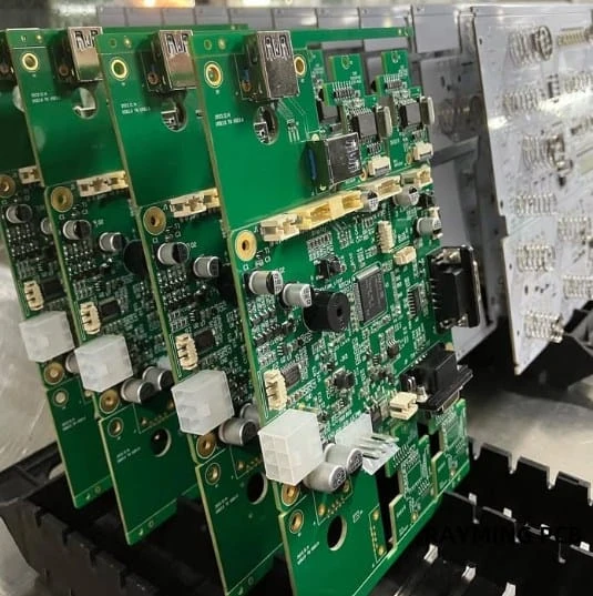
- PCB Assembly Services – Understand how we handle the assembly of fine-pitch GaN components after fabrication.
Request a quote (Design for Manufacturability (DFM) review + pricing)
Ready to move from design to production? Submit your data to APTPCB for a comprehensive DFM review and pricing. We check your stackup against our material stock and validate your impedance calculations before you pay.
Please provide the following for an accurate quote:
- Gerber Files: RS-274X or ODB++.
- Stackup Drawing: Including material type and target impedance.
- Volume: Prototype quantity vs. production volume.
- Testing Requirements: Specify if TDR reports or IPC Class 3 is required.
Conclusion (next steps)
Successfully deploying Gallium Nitride technology requires more than just selecting the right transistor; it demands a holistic approach to GaN power stage PCB impedance control. By defining tight specifications for materials and stackups, understanding the manufacturing risks, and enforcing a strict validation plan, you ensure your power stage performs efficiently and reliably. Use the checklist provided to vet your suppliers and ensure they can meet the rigorous demands of high-speed GaN switching.