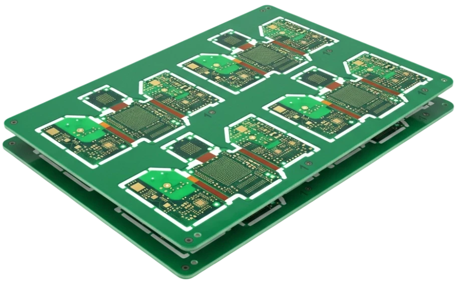
A Hazardous Location PCB is designed to operate safely in environments containing explosive gases, combustible dust, or ignitable fibers without becoming an ignition source. These boards require strict adherence to thermal limits, specific creepage distances, and robust encapsulation to meet standards like ATEX, IECEx, or UL 913. Engineers must prioritize failure containment and thermal management over standard density optimization to ensure safety in critical industrial or architectural applications.
Quick Answer (30 Seconds)
- Core Rule: Maintain a Comparative Tracking Index (CTI) of ≥ 600V (PLC 0) for laminates to prevent electrical tracking in conductive dust environments.
- Critical Range: Keep maximum surface temperature at least 5°C to 10°C below the auto-ignition temperature of the specific gas/dust class (e.g., T4 rating requires < 135°C).
- Verification: Use thermal imaging during load testing to verify no component exceeds the rated Temperature Class (T-Class).
- Common Pitfall: Ignoring "pollution degree" in creepage calculations; dust accumulation can bridge conductors if spacing is based solely on clean lab conditions.
- Boundary Case: In Intrinsic Safety (IS) designs, a single Zener diode is often insufficient; redundant clamping components are required to handle two concurrent faults.
- DFM Tip: Specify "tented and plugged vias" to prevent solder wicking or voids that could compromise insulation barriers or conformal coating integrity.
Highlights
- Safety First: Design strategies for Intrinsic Safety (IS) versus Explosion-Proof encapsulation.
- Material Specs: Why High-Tg (>170°C) and High-CTI materials are non-negotiable.
- Spacing Rules: Concrete creepage and clearance values for 60V–250V systems.
- Coating: The role of conformal coating (25–75 µm) in preventing arcing.
- Testing: How to validate thermal performance and dielectric strength.
- Applications: From industrial sensors to Architectural Light PCB units in harsh zones.
Contents
- Definition and Scope (What It Is, What It Isn’t)
- Rules and Specifications (Key Parameters and Limits)
- Implementation Steps (Process Checkpoints)
- Troubleshooting (Failure Modes and Fixes)
- How to Choose (Design Decisions and Trade-Offs)
- FAQ (Cost, Lead Time, Materials, Testing, Acceptance Criteria)
- Glossary (Key Terms)
- Request a Quote (DFM Review + Pricing)
- Conclusion
Definition and Scope (What It Is, What It Isn’t)
A Hazardous Location PCB is an electronic assembly engineered to prevent the release of sufficient electrical or thermal energy to ignite a hazardous atmosphere. This applies to industries ranging from petrochemical refining to grain processing, and increasingly to Building Integration PCB systems where sensors or lighting are embedded in operational industrial zones.
Applies when:
- The environment contains flammable gases (Class I), combustible dusts (Class II), or ignitable fibers (Class III).
- The device requires certification under UL 913, UL 1203, IEC 60079 (ATEX/IECEx), or CSA C22.2.
- The design strategy relies on Intrinsic Safety (limiting energy), Non-Incendive circuits (no arcs in normal operation), or Encapsulation (potting).
- Operating temperatures are critical; the board must not become a hot spot.
- Reliability is paramount; failure could result in catastrophic explosions, not just device downtime.
Doesn’t apply when:
- The device is located in a "General Purpose" unclassified area (e.g., a standard office server room).
- The enclosure is fully purged and pressurized with clean air (though the PCB inside should still be robust, the strict IS rules may be relaxed).
- Standard consumer electronics (IP ratings like IP67 protect against water/dust ingress but do not guarantee explosion protection).
- High-voltage transmission equipment where arcing is managed by oil or SF6 gas, rather than PCB-level design.
Rules and Specifications (Key Parameters and Limits)
Designing for hazardous locations requires strict adherence to material properties and geometric spacing. The following table outlines critical parameters.
| Rule | Recommended Value/Range | Why It Matters | How to Verify | If Ignored |
|---|---|---|---|---|
| Laminate CTI | ≥ 600V (PLC 0) | Prevents "tracking" (conductive paths) on the surface under voltage stress and contamination. | Check datasheet for ASTM D3638 or IEC 60112 rating. | Carbon tracks form, leading to short circuits and potential ignition. |
| Glass Transition (Tg) | > 170°C (High Tg) | Ensures mechanical stability and Z-axis reliability at elevated operating temperatures. | TMA (Thermomechanical Analysis) verification of material batch. | Pad cratering or barrel cracks occur during thermal cycling. |
| Creepage Distance | ≥ 3.0 mm (for < 60V) | Prevents arcing across the surface, especially in Pollution Degree 3 (industrial) environments. | CAD Design Rule Check (DRC) and physical measurement. | Arcing can occur if dust/moisture bridges the gap, igniting the atmosphere. |
| Clearance Distance | ≥ 2.0 mm (general) | Prevents arcing through the air between conductive parts. | CAD DRC; verify against IPC-2221B or IEC 60079-11 tables. | Sparkover occurs during voltage spikes or transients. |
| Conformal Coating | 25 µm – 75 µm | Provides a dielectric barrier against moisture and conductive dust. | UV inspection (if tracer used) or wet film gauge. | Corrosion or dendrite growth bridges conductors. |
| Copper Weight | ≥ 2 oz (70 µm) | Improves heat dissipation to keep surface temperature low. | Microsection analysis (cross-section). | Traces overheat, exceeding the T-Class limit (e.g., >135°C). |
| Dielectric Strength | > 30 kV/mm | Ensures insulation layers do not break down under high voltage. | Hi-Pot testing (Dielectric Withstand Voltage). | Internal layer shorts leading to catastrophic board failure. |
| Max Surface Temp | < 80% of Auto-Ignition | The hottest component must never ignite the surrounding gas/dust. | Thermal camera imaging under max load + ambient offset. | Device fails certification; high risk of explosion. |
| Void-Free Potting | 100% Fill | If encapsulated, air bubbles can allow gas accumulation and internal ignition. | X-Ray inspection of the potted assembly. | Internal explosion blows apart the casing. |
Implementation Steps (Process Checkpoints)
Building a Hazardous Location PCB involves more than just standard fabrication. It requires a "safety by design" approach.
Select the Protection Method
- Decide if the circuit will be Intrinsically Safe (IS), Encapsulated (m), or Non-Incendive (n).
- Check: For IS, ensure total capacitance and inductance are below the ignition curves for the specific gas group (e.g., Group IIC for Hydrogen).
Material Selection
- Choose a laminate with High Tg (>170°C) and High CTI (>600V).
- Check: Verify the material datasheet explicitly states these values. Consult Isola PCB materials for suitable options.
Component Placement and Thermal Layout
- Space out heat-generating components to avoid hot spots. Use thermal vias and heavy copper planes.
- Check: Run a thermal simulation. Ensure no point exceeds the T-Class limit (e.g., T4 = 135°C, T6 = 85°C).
Routing for Creepage and Clearance
- Set CAD rules to enforce minimum spacing based on IEC 60079-11 (typically stricter than IPC-2221).
- Check: Perform a specific "safety spacing" DRC. Pay attention to spacing under components like optocouplers.
Fabrication with Strict Tolerances
- Ensure etching tolerances do not reduce trace width/spacing below safety limits.
- Check: Request First Article Inspection to measure actual trace widths and spacing.
Assembly and Cleanliness
- Flux residues can be conductive and hygroscopic. Thorough cleaning is mandatory before coating.
- Check: Perform Ionic Contamination testing (ROSE test). Limit should be < 1.56 µg/cm² NaCl equivalent.
Conformal Coating or Potting
- Apply PCB Conformal Coating (Type UR, AR, or SR) or epoxy potting.
- Check: Verify thickness and coverage, especially on sharp edges and component leads.
Final Verification Testing
- Conduct functional tests and specific safety tests (e.g., 500V isolation test for IS circuits).
- Check: Ensure the Quality System records trace these tests to specific serial numbers.
Troubleshooting (Failure Modes and Fixes)
Failures in hazardous locations can be subtle but dangerous. Here is how to diagnose and fix common issues.
Symptom: Arcing or Sparking between Traces
- Likely Cause: Insufficient creepage distance for the pollution degree; conductive dust accumulation; coating voids.
- Checks: Inspect under magnification for carbon tracks (dendrites). Check coating integrity under UV light.
- Fix: Clean the board thoroughly. Re-apply coating with better edge coverage.
- Prevention: Increase spacing in the design phase. Use a slot (milling) between high-voltage pads to increase creepage path.
Symptom: Thermal Shutdown or Hot Spots
- Likely Cause: Undersized traces for the current; poor thermal path to heatsink; component failure.
- Checks: Use a thermal camera. Verify copper weight (is it 1oz instead of the specified 2oz?).
- Fix: Add external heatsinking if possible.
- Prevention: Use Heavy Copper PCB technology. Increase trace width. Use thermal vias connected to ground planes.
Symptom: Coating Delamination
- Likely Cause: Poor surface preparation; flux residue; incompatible coating material.
- Checks: Tape test (cross-hatch adhesion test). Look for "blistering" or "orange peel" effect.
- Fix: Strip and re-coat (difficult). Usually requires scrapping the unit.
- Prevention: Implement strict washing/drying cycles before coating. Ensure compatibility between solder mask and conformal coating.
Symptom: Failed Dielectric Withstand (Hi-Pot) Test
- Likely Cause: Inner layer spacing too tight; voids in the laminate; pre-preg starvation.
- Checks: Cross-section analysis to look for inner layer defects.
- Fix: None for the finished board.
- Prevention: Review PCB Stack-up and dielectric thickness. Ensure pre-preg selection provides adequate resin fill.
Symptom: Component Corrosion in Field
- Likely Cause: Ingress of corrosive gases (H2S, Cl2) through pinholes in coating.
- Checks: Visual inspection for green/black corrosion products on leads.
- Fix: Replace unit.
- Prevention: Switch to a more robust coating (e.g., Parylene) or full potting.
How to Choose (Design Decisions and Trade-Offs)
Making the right design choices early saves certification costs later.
If the environment is Zone 0 (Continuous Hazard)...
- Choose: Intrinsic Safety (Ex ia). The PCB must limit energy under two fault conditions.
- Trade-off: Limits available power significantly. Complex design with redundant Zener barriers.
If the environment is Zone 1 or 2 (Intermittent Hazard)...
- Choose: Flameproof (Ex d) enclosure or Encapsulation (Ex m).
- Trade-off: The PCB can run higher power, but the enclosure is heavy and expensive. The PCB must fit in restricted spaces.
If high power is required (e.g., Motor Drives)...
- Choose: Industrial Control PCB standards with Purged/Pressurized (Ex p) enclosures.
- Trade-off: Requires external air supply and monitoring systems.
If space is extremely limited (e.g., Portable Gas Detectors)...
- Choose: Rigid-Flex PCB to eliminate connectors (which are potential spark points).
- Trade-off: Higher manufacturing cost, but higher reliability.
If the application is Architectural Light PCB...
- Choose: LED boards with Aluminum or Metal Core PCB bases for maximum heat dissipation.
- Trade-off: Single-layer limitations usually apply; complex routing requires careful planning.
If the environment involves corrosive chemicals...
- Choose: Gold surface finish (ENIG or Hard Gold) and thick conformal coating.
- Trade-off: Higher cost than HASL, but prevents contact oxidation.
FAQ (Cost, Lead Time, Materials, Testing, Acceptance Criteria)
Q: How much more does a Hazardous Location PCB cost compared to a standard PCB?
- Typically 20% to 50% higher.
- Costs are driven by high-performance materials (High Tg/CTI), stricter tolerance controls, and mandatory testing (Hi-Pot, ionic cleanliness).
Q: Can I use standard FR-4 for hazardous locations?
- Yes, but with caveats.
- It must be a high-quality FR-4 with a known CTI (Comparative Tracking Index) and appropriate Tg. Generic, low-cost FR-4 often lacks the tracking resistance required for certification.
Q: What is the lead time for these boards?
- Standard lead times apply (e.g., 5–10 days for prototypes), but allow extra time for coating and testing.
- If special laminates (e.g., Rogers or specific Isola grades) are needed, material procurement may add 1–2 weeks.
Q: Do I need special certification to manufacture these PCBs?
- The PCB manufacturer needs a robust Quality Management System (ISO 9001).
- However, the final assembly usually holds the ATEX/UL certification. The PCB fab house must provide a Certificate of Conformance (CoC) proving materials and specs were met.
Q: What is the most critical test for these PCBs?
- Dielectric Withstand Voltage (Hi-Pot) and Ionic Contamination testing.
- Hi-Pot ensures insulation integrity; cleanliness testing ensures no conductive residues remain under the coating.
Q: How does "Building Integration PCB" relate to hazardous locations?
- Modern buildings often integrate sensors and lighting into infrastructure.
- If these are installed in boiler rooms, parking garages (exhaust fumes), or industrial zones, they may require HazLoc ratings.
Q: What surface finish is best?
- ENIG (Electroless Nickel Immersion Gold) is preferred.
- It offers a flat surface for tight-pitch components and excellent corrosion resistance compared to HASL.
Q: Can you repair a Hazardous Location PCB?
- Generally, no.
- Repairs can compromise the conformal coating or the intrinsic safety properties. Most certified devices are "replace only."
Glossary (Key Terms)
| Term | Meaning | Why it matters in practice |
|---|---|---|
| Intrinsic Safety (IS) | A protection technique that limits electrical and thermal energy to levels below what is required to ignite a specific hazardous atmospheric mixture. | Allows maintenance on live equipment in hazardous zones; requires strict component spacing and current limiting. |
| CTI (Comparative Tracking Index) | A measure of the electrical breakdown (tracking) properties of an insulating material. | High CTI materials (PLC 0 or 1) resist carbon tracking, allowing for tighter component spacing. |
| Creepage | The shortest distance between two conductive parts along the surface of the insulation. | Must be sufficient to prevent tracking, especially in dusty/humid environments. |
| Clearance | The shortest distance between two conductive parts through the air. | Prevents spark-over or arcing through the air gap. |
| T-Class (Temperature Class) | A classification system (T1 to T6) indicating the maximum surface temperature a device will generate. | The PCB must stay below the ignition temperature of the gas/dust present (e.g., T6 < 85°C). |
| Zone 0/1/2 | IEC classification for the frequency of hazard presence (0 = continuous, 1 = likely, 2 = unlikely). | Dictates the stringency of the PCB design rules (Zone 0 requires the most robust IS design). |
| Pollution Degree | A rating (1-4) of the amount of dry/wet pollution (dust/moisture) expected in the environment. | Industrial HazLoc PCBs are typically designed for Pollution Degree 3, requiring wider spacing. |
| Conformal Coating | A protective chemical coating or polymer film. | Essential for maintaining dielectric properties and preventing corrosion in harsh environments. |
Request a Quote (DFM Review + Pricing)
To get an accurate quote and a comprehensive Design for Manufacturability (DFM) review for your Hazardous Location PCB, please provide the following details. Our engineering team will review your files against safety standards to ensure compliance.
- Gerber Files: RS-274X or ODB++ format.
- Material Specs: Specify Tg, CTI requirements, and dielectric thickness.
- Stack-up: Detailed layer buildup, especially if impedance or high-voltage isolation is required.
- Surface Finish: Preferred finish (e.g., ENIG, Immersion Silver).
- Coating Requirements: Type of conformal coating and areas to mask (keep-out zones).
- Certification Target: Mention if this is for ATEX, UL 913, or IECEx (helps us check spacing rules).
- Quantities: Prototype vs. Mass Production volumes.
- Special Tests: Hi-Pot voltage levels, Ionic Cleanliness limits, or Impedance Control.
Conclusion
Designing a Hazardous Location PCB is a discipline that balances electrical performance with catastrophic failure prevention. By adhering to strict rules for CTI, creepage, clearance, and thermal management, you ensure your device operates safely in the most volatile environments. Whether for industrial control or specialized Architectural Light PCB applications, selecting the right materials and validating your design through rigorous testing is the only path to certification and safety.