Key Takeaways
- Definition: A Health Monitoring PCB is a specialized circuit board designed to capture, process, and transmit vital physiological or structural data with high precision and reliability.
- Critical Metrics: Signal integrity (low noise), thermal management, and biocompatibility (for wearables) are the non-negotiable performance indicators.
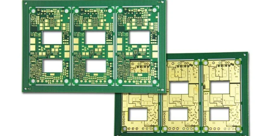
- Material Selection: Standard FR4 is often insufficient; polyimide (Flex) or high-frequency laminates are required for accurate sensor data.
- Misconception: Not all health monitoring is medical; structural health monitoring in aerospace (like an Aircraft Instrument) requires similar durability standards.
- Pro Tip: Always prioritize IPC Class 3 standards for any device where failure could result in loss of data or safety risks.
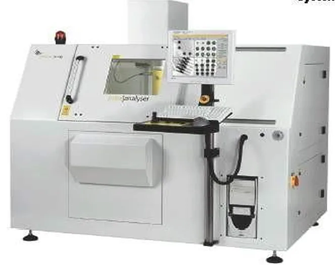
- Validation: Automated Optical Inspection (AOI) is not enough; functional testing and impedance testing are mandatory.
What Health Monitoring PCB really means (scope & boundaries)
Understanding the core definition is the first step before analyzing specific performance metrics. A Health Monitoring PCB is not limited to a single industry; it refers to the electronic backbone of any device responsible for tracking the status of a biological or mechanical system.
In the medical sector, these PCBs drive patient monitoring systems, wearable fitness trackers, and implantable devices. They must handle low-level analog signals from sensors and convert them into digital data without interference.
In the industrial and aerospace sectors, "health monitoring" refers to Structural Health Monitoring (SHM). For example, an Aircraft Display PCB often integrates with sensors that monitor the structural integrity of the fuselage or the performance of an engine. Whether the "patient" is a human or an Aircraft Instrument, the PCB requirements are strikingly similar: extreme reliability, resistance to environmental stress, and zero tolerance for signal latency.
APTPCB (APTPCB PCB Factory) categorizes these boards based on their failure consequence. If a board fails in a consumer toy, it is an inconvenience. If a Health Monitoring PCB fails, it can mean a misdiagnosis or a safety hazard. Therefore, the scope of this guide covers high-reliability boards designed for critical data acquisition.
Health Monitoring PCB metrics that matter (how to evaluate quality)
Once you understand the scope of these high-reliability boards, you must define the metrics that determine their success or failure. Unlike standard consumer electronics, where cost is often the primary driver, health monitoring prioritizes signal fidelity and stability.
The following table outlines the critical metrics designers and procurement teams must track.
| Metric | Why it matters | Typical range or influencing factors | How to measure |
|---|---|---|---|
| Signal-to-Noise Ratio (SNR) | Bio-signals and structural vibration signals are often weak. High noise corrupts data. | Target > 100dB for precision medical audio/sensing. Influenced by trace routing and grounding. | Oscilloscope analysis during Functional Circuit Test (FCT). |
| Leakage Current | Critical for patient safety (medical) and battery life (wearables). | Must be < 10µA for cardiac contact devices (Type CF). | Dielectric Withstand Voltage test (Hi-Pot). |
| Thermal Coefficient of Expansion (CTE) | Mismatched expansion causes solder joint cracks during thermal cycling. | Z-axis expansion should be low (< 50 ppm/°C). Critical for Aircraft Display PCB units exposed to altitude changes. | Thermal Mechanical Analysis (TMA). |
| Impedance Control | Ensures high-speed data from sensors reaches the processor without reflection. | Typically 50Ω (single) or 100Ω (differential) ±10%. | Time Domain Reflectometry (TDR) coupons. |
| Moisture Absorption | Moisture changes dielectric constant, affecting sensor accuracy. | < 0.1% for high-reliability applications. | Weight gain analysis after humidity exposure. |
| Flexural Strength | Wearables and sensors often require the PCB to bend without breaking traces. | Dependent on Polyimide thickness and copper ductility (RA Copper). | IPC-TM-650 Bend Testing. |
How to choose Health Monitoring PCB: selection guidance by scenario (trade-offs)
Knowing the metrics helps, but the specific application scenario dictates which trade-offs are acceptable during the selection process. A board designed for a disposable patch has vastly different requirements than one inside an avionics bay.
Here is how to choose the right Health Monitoring PCB architecture based on common scenarios.
1. Wearable Vital Signs Monitor (Wrist/Chest)
- Recommendation: Rigid-Flex PCB.
- Trade-off: Higher manufacturing cost vs. superior ergonomics and durability.
- Why: The rigid section houses the MCU and battery, while the flexible tail connects to skin sensors. This eliminates bulky connectors that can fail due to body movement.
2. Implantable Medical Device (Pacemaker/Glucose)
- Recommendation: HDI (High Density Interconnect) with biocompatible materials.
- Trade-off: Extreme miniaturization complexity vs. patient safety.
- Why: Space is premium. You need microvias and fine lines (3/3 mil) to fit complex logic into a tiny footprint. Materials must be non-toxic and stable.
3. Aerospace Structural Health Monitoring (SHM)
- Recommendation: High-Tg Rigid PCB with heavy copper.
- Trade-off: Material cost vs. thermal and vibration resistance.
- Why: An Aircraft Instrument monitoring wing stress faces extreme temperature swings (-55°C to +125°C). Standard FR4 will delaminate. High-Tg materials prevent pad cratering.
4. Hospital Bedside Monitor (Stationary)
- Recommendation: Standard Multilayer Rigid PCB (4-8 layers).
- Trade-off: Size is less critical; focus is on EMI shielding.
- Why: These units operate near other high-power equipment (MRI, X-Ray). Good stackup design with dedicated ground planes is essential to prevent interference.
5. Disposable Diagnostic Patch
- Recommendation: Single or Double-sided Flex (Polyimide or PET).
- Trade-off: Low durability (single use) vs. extremely low cost.
- Why: Cost is the driver. The PCB is often printed with conductive ink or etched on thin substrates to be discarded after 24 hours.
6. High-Frequency Imaging (Ultrasound/MRI)
- Recommendation: Hybrid Stackup (FR4 + Rogers/Teflon).
- Trade-off: Complex lamination process vs. signal clarity.
- Why: High-frequency signals require low-loss materials (Rogers), but the digital logic section can use cheaper FR4. A hybrid board optimizes both cost and performance.
Health Monitoring PCB implementation checkpoints (design to manufacturing)
After selecting the right board type for your scenario, the focus shifts to the execution phase where design files are converted into physical hardware. APTPCB recommends a strict checkpoint system to prevent costly revisions.
The following checkpoints cover the journey from design files to the final product.
Stackup Verification
- Recommendation: Confirm dielectric thickness matches impedance requirements before routing.
- Risk: Incorrect impedance leads to signal reflection and data corruption.
- Acceptance: Manufacturer provides a TDR simulation report matching the design.
Material Certification
- Recommendation: Use UL-certified laminates suitable for the operating environment (e.g., Isola 370HR for reliability).
- Risk: Generic materials may outgas or delaminate under thermal stress.
- Acceptance: Review Material Datasheets and Certificate of Conformance (CoC).
Trace Width and Spacing (DFM)
- Recommendation: Maintain minimum 4-5 mil trace/space for HDI, 6-8 mil for standard.
- Risk: Acid traps or etching issues causing shorts/opens in fine-pitch areas.
- Acceptance: DFM Guidelines check passes with zero critical errors.
Analog/Digital Separation
- Recommendation: Physically separate sensitive analog sensor traces from noisy digital clock lines.
- Risk: Digital noise coupling into the analog signal (crosstalk), rendering health data useless.
- Acceptance: Visual inspection of Gerber files for split ground planes or proper partitioning.
Surface Finish Selection
- Recommendation: Use ENIG (Electroless Nickel Immersion Gold) or ENEPIG.
- Risk: HASL surfaces are uneven, causing placement issues for fine-pitch sensor components.
- Acceptance: Surface flatness measurement and solderability test.
Via Reliability
- Recommendation: Tent or plug vias in critical areas; use filled vias for via-in-pad.
- Risk: Solder wicking away from pads through open vias, leading to weak joints.
- Acceptance: Cross-section analysis (microsection) to verify plating thickness (IPC Class 3 requires average 25µm).
Cleanliness and Ionic Contamination
- Recommendation: Strict washing protocols to remove flux residues.
- Risk: Dendrite growth (electrochemical migration) causing shorts over time, especially in humid environments.
- Acceptance: ROSE testing (Resistivity of Solvent Extract) < 1.56 µg/cm² NaCl equivalent.
Solder Mask Accuracy
- Recommendation: Use Laser Direct Imaging (LDI) for precise mask alignment.
- Risk: Mask slivers bridging pads on fine-pitch sensor ICs.
- Acceptance: Visual inspection ensuring mask expansion is within 2-3 mils.
Fiducial Placement
- Recommendation: Place local fiducials near high-pin-count sensor packages.
- Risk: Pick-and-place machine misalignment.
- Acceptance: Presence of fiducials in assembly drawing and Gerbers.
Final Electrical Test
- Recommendation: 100% Netlist testing (Flying Probe for prototypes, Bed of Nails for mass production).
- Risk: Shipping a board with a latent open circuit.
- Acceptance: Pass/Fail report for every single unit.
Health Monitoring PCB common mistakes (and the correct approach)
Even with a solid plan and strict checkpoints, developers often fall into specific traps that compromise the long-term reliability of the device. Avoiding these pitfalls is essential for maintaining the integrity of a Health Monitoring PCB.
- Mistake 1: Ignoring Thermal Management in Wearables.
- Issue: Designers assume low-power wearables don't get hot. However, skin contact insulates the PCB, trapping heat.
- Correction: Use thermal vias and copper pours to spread heat away from the sensor and battery.
- Mistake 2: Over-specifying the Drill Chart.
- Issue: Using 10 different drill sizes when 4 would suffice increases tooling cost and time.
- Correction: Consolidate drill sizes where possible without violating aspect ratios.
- Mistake 3: Neglecting Flex Points in Rigid-Flex Designs.
- Issue: Placing vias or components near the bend line of a flexible tail.
- Correction: Keep the bend area free of plated holes and ensure traces run perpendicular to the bend.
- Mistake 4: Using Standard HASL for Fine-Pitch Sensors.
- Issue: The uneven surface of Hot Air Solder Leveling prevents BGA or QFN sensors from seating flat.
- Correction: Always specify ENIG for flat, reliable pads.
- Mistake 5: Underestimating Mechanical Stress in Aerospace.
- Issue: Designing an Aircraft Display PCB without considering high-frequency vibration.
- Correction: Add mounting holes and keep heavy components away from the center of the board to reduce harmonic resonance issues.
- Mistake 6: Poor Documentation for Assembly.
- Issue: Sending only Gerbers without a clear assembly drawing or Pick-and-Place file.
- Correction: Provide a complete package including XY coordinates, rotation data, and clear polarity markings.
Health Monitoring PCB FAQ (cost, lead time, materials, testing, acceptance criteria)
To clarify remaining doubts regarding procurement and specification, here are the most frequently asked questions.
1. How does material selection impact Health Monitoring PCB cost? Material is a major cost driver. Standard FR4 is the baseline. Moving to Polyimide (for flex) can increase substrate cost by 2-3x. High-frequency materials like Rogers can increase costs by 5-10x. However, for health monitoring, the cost of failure outweighs the material savings.
2. What is the standard Health Monitoring PCB lead time for prototypes? For standard rigid boards, lead time is typically 3-5 days. For complex Rigid-Flex or HDI boards often used in health devices, expect 8-12 working days due to additional lamination and laser drilling steps.
3. Which Health Monitoring PCB materials are best for skin contact? The PCB itself rarely touches skin directly; it is usually encased. However, if the PCB substrate is exposed (e.g., in a patch), Polyimide is preferred for its flexibility and chemical inertness. The enclosure material is the primary biocompatibility concern.
4. What specific Health Monitoring PCB testing is required for aerospace applications? Beyond standard electrical testing, aerospace boards (like those for an Aircraft Instrument) often require Thermal Cycling (-55°C to +125°C), Vibration Testing, and Burn-in testing to weed out infant mortality failures.
5. What are the Health Monitoring PCB acceptance criteria for IPC Class 3? IPC Class 3 (High Reliability) requires tighter tolerances than Class 2. For example, annular rings must be functional with no breakout allowed (Class 2 allows 90 degrees breakout). Plating thickness in holes must average 25µm (vs 20µm for Class 2).
6. Can APTPCB handle the assembly of sensitive sensor components? Yes. Handling sensitive MEMS sensors or optical sensors requires strict ESD control and precise reflow profiles to avoid damaging the sensing element.
7. How do you ensure data security at the hardware level? While mostly firmware-driven, hardware can support security via dedicated crypto-chips. The PCB design must ensure these chips have tamper-proof routing (e.g., buried traces) to prevent physical probing.
8. Why is impedance control critical for health sensors? Many modern health sensors use high-speed digital interfaces (MIPI, SPI). If the trace impedance doesn't match the source/load (usually 50Ω), signals reflect back, causing "ghosting" or data errors, which looks like noise in the health reading.
Resources for Health Monitoring PCB (related pages and tools)
- Medical PCB Solutions: Deep dive into specific medical standards and capabilities.
- Aerospace & Defense PCB: Information on high-reliability boards for SHM and avionics.
- PCB Quality Control System: Details on how we validate reliability through certifications and testing.
- Rigid-Flex PCB Capabilities: Technical specs for wearable-friendly board architectures.
Health Monitoring PCB glossary (key terms)
| Term | Definition |
|---|---|
| AOI | Automated Optical Inspection. A camera-based check for surface defects like missing components or solder bridges. |
| Biocompatibility | The property of a material being compatible with living tissue; critical for wearables and implants. |
| CTE | Coefficient of Thermal Expansion. How much a material expands when heated. Mismatches cause failure. |
| DFM | Design for Manufacturing. The practice of designing boards that are easy and cheap to manufacture without defects. |
| EMI | Electromagnetic Interference. Radio noise that can disrupt sensor signals. |
| ENIG | Electroless Nickel Immersion Gold. A flat, oxidation-resistant surface finish ideal for sensors. |
| FCT | Functional Circuit Test. Testing the actual operation of the board (power up, signal check) rather than just continuity. |
| HDI | High Density Interconnect. PCBs with microvias and fine lines, used to miniaturize health devices. |
| IPC Class 3 | The highest reliability standard for PCBs, used for life-support and aerospace systems. |
| Microvia | A very small laser-drilled hole (typically < 6 mil) used to connect layers in HDI boards. |
| Rigid-Flex | A hybrid PCB construction combining rigid FR4 sections with flexible polyimide tails. |
| SHM | Structural Health Monitoring. Using sensors and PCBs to monitor the physical condition of machines or aircraft. |
| Signal Integrity | The quality of an electrical signal. Good integrity means clean, noise-free data. |
Conclusion (next steps)
Developing a Health Monitoring PCB requires a shift in mindset from "consumer electronics" to "mission-critical reliability." Whether you are designing a next-generation heart monitor or an Aircraft Display PCB for cockpit alerts, the fundamentals remain the same: precise material selection, rigorous impedance control, and uncompromising testing standards.
APTPCB specializes in bridging the gap between complex design requirements and manufacturability. To move your project forward, prepare the following for a comprehensive DFM review and quote:
- Gerber Files (RS-274X): The blueprint of your design.
- Fabrication Drawing: Specifying IPC Class (2 or 3), materials, and stackup.
- BOM (Bill of Materials): If assembly is required, include specific sensor part numbers.
- Test Requirements: Define if you need ICT, FCT, or specific impedance reporting.
Reliability starts at the design stage. Ensure your health monitoring device is built on a foundation of quality.