Healthcare Light PCB technology demands far stricter adherence to reliability and safety standards than standard commercial lighting. Whether used in surgical theater lamps, diagnostic imaging backlights, or patient room circadian lighting, the printed circuit board serves as the thermal and electrical backbone of the medical device. Engineers must balance high thermal conductivity with rigorous dielectric breakdown voltage requirements to ensure patient safety and device longevity.
APTPCB (APTPCB PCB Factory) specializes in manufacturing high-reliability metal core and rigid PCBs for the medical sector. This guide provides the technical specifications, failure analysis protocols, and design rules necessary to engineer robust Healthcare Light PCBs that meet IEC 60601 standards and thermal performance targets.
Healthcare Light PCB quick answer (30 seconds)
For engineers designing medical illumination systems, the PCB is the critical thermal path. Here are the core requirements:
- Thermal Conductivity: Most medical LED applications require Metal Core PCBs (MCPCB) with a dielectric thermal conductivity of 2.0 W/mK to 5.0 W/mK to manage high-power LED heat flux.
- Dielectric Breakdown Voltage: Safety standards often dictate a breakdown voltage (Hi-Pot) of >3000V AC or even >5000V AC between the circuit and the metal base, significantly higher than the 1000V typical in consumer lighting.
- Solder Mask Reflectivity: Use specific high-reflectivity white solder masks (reflectivity >90%) to maximize lumen output and maintain Color Rendering Index (CRI) stability.
- Surface Finish: ENIG (Electroless Nickel Immersion Gold) or ENEPIG is preferred over HASL to ensure flat pads for fine-pitch LEDs and wire bonding reliability in high-end modules.
- Material Stability: The substrate must resist yellowing and degradation under continuous UV exposure if UV-C disinfection LEDs are mounted.
- Trace Thickness: Heavy copper (2oz or 3oz) is frequently required to minimize voltage drop across long LED strings, ensuring uniform brightness across large surgical arrays.
When Healthcare Light PCB applies (and when it doesn’t)
Medical lighting is a broad category, but "Healthcare Light PCB" specifically refers to critical illumination systems where failure or performance degradation poses a risk to clinical outcomes.
Applies to:
- Surgical Lighting: High-intensity, shadow-less lamps requiring extreme thermal management to prevent LED junction overheating and color shift.
- Diagnostic Imaging: Backlighting for X-ray film viewers or MRI-compatible lighting (requiring non-magnetic materials).
- Endoscopic Illumination: Miniature rigid or flex PCBs carrying high-power micro-LEDs at the tip of medical instruments.
- UV Disinfection Units: PCBs carrying UV-C LEDs for sterilizing operating rooms or equipment, requiring UV-resistant solder masks.
- Patient Monitoring Indicators: High-reliability status lights on life-support equipment.
Does not apply to (Standard Commercial Specs):
- General Hallway Lighting: While hospitals use it, standard Architectural Light PCB specs (FR4, 1oz copper) are usually sufficient unless specific fire ratings are required.
- Administrative Office Lighting: Standard commercial LED strips are cost-effective here.
- Parking Lot Lighting: Standard Flood Light PCB designs work here, focusing on weatherproofing rather than medical-grade electrical isolation.
- Decorative Lobby Lighting: Unless integrated into a medical alert system, standard Facade Light PCB or Cove Light PCB technologies apply.
Healthcare Light PCB rules and specifications (key parameters and limits)
The following table outlines the critical design parameters for Healthcare Light PCBs. Deviating from these ranges often leads to thermal runaway or safety compliance failures.
| Rule / Parameter | Recommended Value / Range | Why it matters | How to verify | If ignored (Risk) |
|---|---|---|---|---|
| Base Material | Aluminum (5052/6061) or Copper | Provides the primary heat sink path. Copper is used for extreme power density. | Material certification (C of C), XRF analysis. | LED overheating, rapid lumen depreciation. |
| Dielectric Thermal Conductivity | 2.0 W/mK – 8.0 W/mK | Transfers heat from LED pad to metal base through the insulating layer. | ASTM D5470 testing. | Junction temperature ($T_j$) exceeds limits; LED failure. |
| Dielectric Thickness | 38µm – 150µm | Balances thermal transfer (thinner is better) vs. electrical isolation (thicker is better). | Cross-section analysis (microsection). | Hi-Pot failure (too thin) or overheating (too thick). |
| Breakdown Voltage (Hi-Pot) | >3000V AC (up to 6kV) | Prevents arcing from traces to the metal chassis, crucial for patient safety (IEC 60601). | Hi-Pot tester (Dielectric Withstand Test). | Electric shock hazard; failed safety certification. |
| Copper Weight | 2oz – 4oz (70µm – 140µm) | Reduces $I^2R$ losses and spreads heat laterally before it passes through the dielectric. | Microsection or resistance measurement. | Voltage drop causes dimming at end of strings; localized hot spots. |
| Solder Mask Color | Super White / High Reflectivity | Maximizes light output; standard green absorbs light and shifts color temperature. | Spectrophotometer (Reflectivity %). | Reduced efficiency; potential color shift in surgical fields. |
| Surface Finish | ENIG / Immersion Silver | Provides flat surface for LED thermal pads; prevents oxidation affecting thermal transfer. | X-Ray Fluorescence (XRF). | Poor solder joints; high thermal resistance at solder interface. |
| Glass Transition Temp (Tg) | >130°C (for dielectric) | Ensures the dielectric layer does not soften under operating thermal load. | TMA (Thermal Mechanical Analysis). | Delamination of copper from dielectric during operation. |
| Peel Strength | >1.0 N/mm | Ensures copper traces do not lift under thermal cycling stress. | Peel strength tester. | Open circuits after repeated power cycles. |
| Warpage / Bow & Twist | <0.5% | Critical for attaching the PCB flat against the heat sink housing. | Flatness gauge / Laser profilometer. | Air gaps between PCB and heat sink; catastrophic thermal failure. |
Healthcare Light PCB implementation steps (process checkpoints)
Manufacturing a reliable Healthcare Light PCB involves specific steps to ensure thermal performance and electrical isolation.
Thermal Simulation and Stack-up Design
- Action: Before layout, simulate the heat flux based on LED wattage and density. Select the dielectric conductivity (e.g., 2W vs 4W) based on the simulation.
- Key Parameter: Max Junction Temperature ($T_j$) < 85°C (or LED mfr spec).
- Check: Verify that the theoretical thermal resistance ($R_{th}$) meets the cooling budget.
Material Selection and Procurement
- Action: Choose the metal base (Aluminum 5052 for general, 6061 for hardness, Copper for high performance). Specify the UL-rated dielectric layer.
- Key Parameter: CTI (Comparative Tracking Index) > 600V (PLC 0).
- Check: Review material datasheets for UL 94 V-0 flammability rating.
Circuit Patterning and Etching
- Action: Etch the copper circuit. For heavy copper (>2oz), apply compensation factors to trace widths to account for undercutting.
- Key Parameter: Trace width tolerance ±10% (standard) or ±5% (precision).
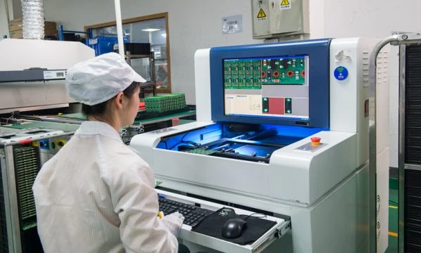
- Check: Automated Optical Inspection (AOI) to detect opens, shorts, or "neck-downs" in high-current paths.
Solder Mask Application
- Action: Apply high-reflectivity white solder mask. Ensure the mask does not encroach on the LED thermal pad (solder mask defined vs. non-solder mask defined pads).
- Key Parameter: Mask thickness over copper >10µm.
- Check: Visual inspection for coverage and alignment; reflectivity check.
Surface Finish Deposition
- Action: Apply ENIG or Immersion Silver. HASL is generally avoided for high-power LEDs due to uneven surfaces causing LED tilt.
- Key Parameter: Gold thickness 1-3µin (for ENIG).
- Check: XRF measurement of coating thickness.
Mechanical Routing and V-Scoring
- Action: Cut the individual boards or panels. For metal core boards, specialized carbide cutters or diamond blades are used to prevent burrs.
- Key Parameter: Burr height <50µm.
- Check: Visual inspection of edges; verify V-score depth allows for clean separation without bending the metal.
Electrical Safety Testing (Hi-Pot)
- Action: Apply high voltage between the circuit network and the metal base to test dielectric integrity.
- Key Parameter: No leakage current >1mA at specified voltage (e.g., 2000V).
- Check: 100% electrical test pass/fail log.
Solder Paste Printing and Assembly (PCBA)
- Action: Use a stencil designed with appropriate aperture reduction (e.g., 60-70% coverage on thermal pads) to prevent solder voiding.
- Key Parameter: Solder void percentage <25% (or stricter <10% for medical).
- Check: X-Ray inspection of the thermal pad solder joint.
Reflow Soldering
- Action: Use a profile optimized for the high thermal mass of the metal core PCB. The soak time may need to be longer to bring the aluminum base up to temp.
- Key Parameter: Time Above Liquidus (TAL) 45-90 seconds.
- Check: Profiling with thermocouples attached to the metal base.
Final Functional and Burn-in Testing
- Action: Power up the module and run for a set period (e.g., 24 hours) to screen for infant mortality.
- Key Parameter: Stable current draw and temperature.
- Check: Thermal imaging to identify hot spots indicating poor solder joints or die attach issues.
Healthcare Light PCB troubleshooting (failure modes and fixes)
When Healthcare Light PCBs fail, the root cause is often thermal or mechanical. Use this guide to diagnose issues.
Symptom 1: LED Color Shift (Blue shift or yellowing)
- Causes: Excessive junction temperature ($T_j$) degrading the phosphor; chemical incompatibility with solder mask fumes.
- Checks: Measure case temperature ($T_c$) at the solder point. Check for discoloration of the solder mask.
- Fix: Increase dielectric thermal conductivity (e.g., switch from 1W to 3W). Switch to a chemical-resistant solder mask.
- Prevention: Perform chemical compatibility testing between LEDs, mask, and conformal coatings.
Symptom 2: Intermittent Operation or Flickering
- Causes: Cracked solder joints due to thermal expansion mismatch (CTE mismatch) between the ceramic LED and the metal PCB.
- Checks: Microsection the solder joint. Look for fatigue cracks.
- Fix: Use a dielectric with a lower modulus (softer) to absorb stress. Optimize the solder stencil design to ensure a thicker bond line.
- Prevention: Conduct thermal shock cycling tests (-40°C to +125°C) during qualification.
Symptom 3: Hi-Pot (Dielectric Withstand) Failure
- Causes: Burrs from mechanical routing piercing the dielectric; insufficient creepage distance at board edges; voids in the dielectric material.
- Checks: Inspect board edges under a microscope for metal burrs. X-ray the dielectric for voids.
- Fix: Increase "copper-to-edge" clearance (pullback). Improve routing bit maintenance. Use higher voltage-rated dielectric material.
- Prevention: Set strict burr height limits and copper pullback rules (typically >0.5mm pullback).
Symptom 4: PCB Delamination / Blistering
- Causes: Moisture absorption in the dielectric followed by reflow (popcorn effect); overheating during operation.
- Checks: Check if boards were baked before reflow. Inspect for bubbles under the copper.
- Fix: Bake PCBs to remove moisture before assembly. Ensure reflow profile peak temperature does not exceed material limits.
- Prevention: Store PCBs in vacuum-sealed bags with desiccant.
Symptom 5: Uneven Brightness Across the Array
- Causes: Voltage drop ($IR$ drop) in the copper traces due to insufficient width or thickness.
- Checks: Measure voltage at the first and last LED in the string.
- Fix: Increase copper weight (e.g., 1oz to 2oz). Widen power traces.
- Prevention: Calculate trace resistance during layout phase.
Symptom 6: High Thermal Resistance ($R_{th}$) Measurements
- Causes: Poor wetting of the thermal pad; voids in the solder interface; dielectric thickness out of spec.
- Checks: X-ray inspection for voiding percentage. Cross-section to verify dielectric thickness.
- Fix: Adjust stencil aperture for the thermal pad (window pane design).
- Prevention: Optimize reflow profile for high-mass boards.
How to choose Healthcare Light PCB (design decisions and trade-offs)
Choosing the right PCB configuration involves balancing cost, thermal performance, and mechanical constraints.
1. Metal Core (MCPCB) vs. FR4 with Thermal Vias
- Decision: Use MCPCB for high-power LEDs (>1W) or high-density arrays (Surgical lights). The aluminum base acts as a heat spreader.
- Decision: Use FR4 with Thermal Vias for low-power indicators or when complex multi-layer routing is required (e.g., control boards with integrated LEDs).
- Trade-off: MCPCB offers superior cooling but is typically limited to 1 or 2 layers. FR4 allows many layers but has poor thermal conductivity (0.3 W/mK) unless heavily plated with vias.
2. Aluminum vs. Copper Base
- Decision: Aluminum is the industry standard—lightweight and cost-effective.
- Decision: Copper is used for extreme power density (e.g., UV curing or high-intensity laser diodes) because copper conducts heat (390 W/mK) better than aluminum (170-200 W/mK).
- Trade-off: Copper is significantly heavier and more expensive.
3. Dielectric Layer Selection
- Decision: Standard Dielectric (1-2 W/mK) is sufficient for general ward lighting or Cove Light PCB applications.
- Decision: High-Performance Dielectric (3-8 W/mK) is mandatory for surgical theater lights to maintain stable CRI and prevent premature failure.
- Trade-off: Higher conductivity dielectrics are more expensive and can be more brittle.
4. Comparison with Other Lighting Types
- vs. Architectural Light PCB: Healthcare PCBs require higher CRI consistency and stricter safety isolation. Architectural boards prioritize cost and form factor.
- vs. Flood Light PCB: Both use MCPCBs, but Healthcare PCBs often require smoother surface finishes (ENIG) for precision LEDs, whereas outdoor floodlights might use HASL.
- vs. Education Light PCB: Lighting for classrooms focuses on low glare (UGR). Healthcare lighting focuses on biological safety and accurate color rendering for diagnosis.
Healthcare Light PCB FAQ (cost, lead time, common defects, acceptance criteria, Design for Manufacturability (DFM) files)
Q: What is the typical lead time for custom Healthcare Light PCBs? A: Standard MCPCB prototypes typically take 3-5 days. Mass production takes 10-15 days. If special high-conductivity dielectric materials (e.g., 5W/mK or higher) are required, lead times may extend by 1-2 weeks depending on material stock.
Q: How does the cost of Healthcare Light PCB compare to standard FR4? A: Healthcare Light PCBs (MCPCBs) are generally 2-3x more expensive per square inch than simple FR4 due to the aluminum/copper base and specialized dielectric. However, they eliminate the need for large additional heat sinks, often lowering the total system cost.
Q: What files are required for a DFM review? A: You must provide Gerber files (RS-274X), a drill file, and a fabrication drawing specifying the material stack-up (dielectric thickness/conductivity), aluminum alloy type, solder mask color, and breakdown voltage requirements. For assembly, a Pick & Place file and BOM are needed.
Q: Can you manufacture "Bendable" Aluminum PCBs for curved medical fixtures? A: Yes. We can use a specific aluminum alloy (like 5052) and a flexible dielectric that allows for slight bending (semi-flex). Alternatively, for tight radii, we recommend Rigid-Flex PCB or segmented MCPCBs joined by wires.
Q: What are the acceptance criteria for solder voids on thermal pads? A: For general lighting, <30% voiding is often acceptable. For Healthcare Light PCBs, specifically high-power surgical nodes, we target <15% or <10% voiding to ensure uniform thermal transfer. This is verified via X-ray inspection.
Q: Do you support UV-C LED boards for sterilization? A: Yes. UV-C radiation degrades standard organic solder masks quickly, causing them to chalk or flake. We use specialized UV-stable solder masks or recommend exposing the metal surface (with appropriate plating) in non-conductive areas to prevent degradation.
Q: How do you handle the "Cove Light PCB" requirements for patient rooms? A: These are often long, narrow boards. We use V-scoring to panelize them efficiently. We ensure color consistency (MacAdam Ellipse steps) by sourcing LEDs from the same bin and using high-reflectivity mask to minimize color shift.
Q: What is the difference between isolation in Facade Light PCB vs. Healthcare Light PCB? A: Facade Light PCB focuses on moisture ingress protection (IP rating). Healthcare Light PCB focuses on electrical isolation (dielectric strength) to prevent shock to patients, even if the device is touched. The testing protocols (Hi-Pot vs. Water Spray) differ significantly.
Q: Can I use heavy copper on a metal core PCB? A: Yes, we can fabricate MCPCBs with up to 4oz or 6oz copper. This is useful for low-voltage, high-current applications to minimize voltage drop. Note that heavy copper requires wider trace spacing (clearance).
Q: What testing standards do you follow? A: We follow IPC-6012 (Class 2 or Class 3 for medical) for PCB fabrication. For assembly, we follow IPC-A-610. We can also support UL certification marking on the PCB if required for your end-device approval.
Q: How do you prevent "Education Light PCB" flicker in medical training rooms? A: Flicker is usually a driver issue, but PCB layout plays a role. We minimize loop inductance in the layout and ensure low-resistance ground paths. We also assist in matching the PCB thermal mass to the driver's feedback loop to prevent thermal oscillation.
Q: Why is the breakdown voltage test failing on my prototypes? A: Common causes include: burrs on the aluminum edge reducing the gap to the copper, copper traces too close to the board edge (violating creepage rules), or using a low-grade dielectric. We recommend a minimum 0.5mm - 1.0mm pullback of copper from the board edge.
Q: Do you offer assembly for these boards? A: Yes, APTPCB provides full turnkey assembly. We have experience handling ceramic-base LEDs and fine-pitch connectors used in medical devices. See our Medical PCB page for more details.
Q: What is the maximum length for a single Healthcare Light PCB? A: We can manufacture boards up to 1200mm or 1500mm long for linear applications (like bed-head units). However, shipping and handling very long MCPCBs requires special crating to prevent bending.
Resources for Healthcare Light PCB (related pages and tools)
- Metal Core PCB Capabilities: Detailed specs on aluminum and copper base materials.
- High Thermal PCB: Solutions for extreme heat management.
- PCB Quality Control: How we verify reliability through microsectioning and electrical testing.
- Medical PCB Industry Page: Specifics on ISO 13485 compliance and medical applications.
- DFM Guidelines: Design rules to ensure your board is manufacturable.
Healthcare Light PCB glossary (key terms)
| Term | Definition | Context in Healthcare Lighting |
|---|---|---|
| MCPCB | Metal Core Printed Circuit Board. | The standard substrate for power LEDs, using a metal base for cooling. |
| Dielectric Layer | The insulating material between the copper circuit and metal base. | The critical component determining thermal conductivity and electrical safety. |
| Thermal Conductivity (W/mK) | A measure of a material's ability to conduct heat. | Higher values (2-5 W/mK) are needed for high-power surgical lights. |
| Breakdown Voltage | The voltage at which the insulation fails and current arcs. | Must be high (>3kV) to meet medical safety standards (IEC 60601). |
| CRI (Color Rendering Index) | A quantitative measure of the ability of a light source to reveal colors faithfully. | Critical in surgery to distinguish tissues; PCB mask color can affect this. |
| Junction Temperature ($T_j$) | The temperature at the core of the LED semiconductor. | Must be kept low via the PCB to prevent failure. |
| IMS | Insulated Metal Substrate. | Another term for MCPCB. |
| Creepage Distance | The shortest path between two conductive parts along the surface of the insulation. | Vital for safety compliance at high voltages. |
| Clearance | The shortest distance between two conductive parts through the air. | Must be maintained to prevent arcing. |
| MacAdam Ellipse | A region on a chromaticity diagram containing all colors indistinguishable to the average human eye. | Used to define LED color binning consistency. |
| Lumen Maintenance | How well a light source maintains its light output over time. | Poor PCB thermal design leads to rapid lumen depreciation. |
| Solder Void | Empty spaces within a solder joint. | Reduces thermal transfer efficiency; critical defect in power LED pads. |
| Heavy Copper | Copper thickness >2oz (70µm). | Used to carry high current with minimal voltage drop. |
Request a quote for Healthcare Light PCB (Design for Manufacturability (DFM) review + pricing)
Ready to manufacture your medical lighting solution? APTPCB provides comprehensive DFM reviews to ensure your design meets thermal and safety requirements before production begins.
What to send for an accurate quote:
- Gerber Files: Including all copper, solder mask, and drill layers.
- Stack-up / Material Spec: Specify Aluminum/Copper base, dielectric conductivity (e.g., 2W/mK), and finished copper weight.
- Drawings: Fabrication drawing showing V-score lines, countersinks, and tolerance requirements.
- Volume: Prototype quantity vs. estimated annual usage.
- Special Requirements: Hi-Pot voltage limits, specific solder mask reflectivity, or UL marking needs.
Conclusion (next steps)
Healthcare Light PCB design is a discipline that merges thermal engineering with strict electrical safety compliance. Whether you are developing high-intensity surgical arrays or ambient patient room lighting, the choice of substrate material, dielectric properties, and manufacturing quality directly impacts patient safety and device certification. By adhering to the specifications for thermal conductivity, breakdown voltage, and surface finish outlined in this guide, engineers can deliver reliable, high-performance medical illumination systems.