
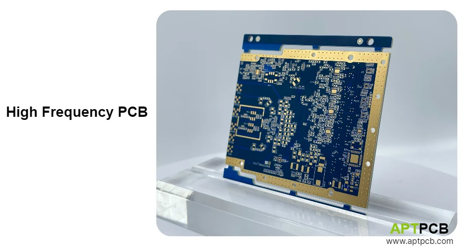
A high-frequency multilayer PCB stack-up is an engineered electrical structure, not only a layer arrangement. RF performance depends on the relationship between laminate selection, dielectric thickness, copper profile, reference planes, via transitions, lamination sequence, and manufacturing controls.
For RF and high-speed designs, the stack-up should be finalized before impedance routing begins. A successful RFQ package defines the electrical targets, construction details, manufacturing processes, and verification evidence required from the PCB supplier.
What information should be defined before selecting a high-frequency PCB stack-up?
The stack-up decision starts with the application requirements:
| Design requirement | Stack-up impact |
|---|---|
| Operating frequency and bandwidth | Determines acceptable dielectric loss, conductor loss, and material selection |
| Impedance target | Defines trace geometry, dielectric thickness, copper thickness, and reference plane location |
| Signal loss budget | Determines laminate Dk, Df, copper roughness, and route-length constraints |
| Layer count and routing density | Controls signal layers, plane placement, HDI requirements, and via structures |
| Power integrity requirements | Defines plane pairing, decoupling strategy, and switching-current containment |
| Mechanical requirements | Influences board thickness, copper balance, symmetry, and lamination approach |
A stack-up that works electrically in simulation must also be manufacturable with stable dielectric thickness, registration, plating, and material availability.
How should RF, digital, power, and analog layers be arranged?
A high-frequency multilayer PCB should separate functional zones while maintaining continuous return paths.
| Zone | Preferred stack-up treatment | Key interaction |
|---|---|---|
| RF/microwave | Low-loss material near a solid reference | Bonding, copper profile, launch and via geometry |
| High-speed digital | Controlled impedance routing with continuous references | Crosstalk, via stubs and plane transitions |
| Sensitive analog/clock | Quiet reference structures | Power noise and isolation |
| Power conversion | Short current loops and thermal copper | EMI coupling into RF and digital areas |
| High-current distribution | Heavy copper or dedicated planes | Copper balance and thermal expansion |
A symmetric-looking stack-up is not automatically electrically or mechanically balanced. Copper distribution, resin flow, dielectric variation, and material combinations influence registration and warpage.
When should a hybrid RF PCB stack-up be used?
Hybrid stack-ups combine high-performance RF materials with standard PCB materials to place expensive laminate only where electrical performance requires it.
A typical hybrid decision looks like this:
| Construction option | Best fit | Design consideration |
|---|---|---|
| All FR-4 construction | Lower-frequency designs with short routes | Cost-effective but may have higher loss |
| Full RF laminate construction | Broad RF coverage or very low-loss requirements | Higher material cost |
| Hybrid RF/FR-4 construction | Mixed RF, digital, and power systems | Requires lamination, CTE, and adhesion validation |
Hybrid designs require coordination between materials because different laminates may have different:
- dielectric constants;
- dissipation factors;
- resin systems;
- thermal expansion behavior;
- lamination pressures;
- drilling and desmear requirements.
Before release, confirm:
- exact core, prepreg, and bond-ply families;
- pressed dielectric thickness;
- copper foil type and profile;
- lamination temperature compatibility;
- sequential lamination cycle count;
- registration capability;
- impedance coupon construction.
Which PCB materials should be specified for high-frequency designs?
Material selection should match the loss budget rather than frequency alone.
Specify the complete material construction, including grade and thickness. Examples include Rogers RO4350B 10 mil or equivalent approved materials when the design requires controlled dielectric behavior.
Important material parameters include:
| Parameter | Why it matters |
|---|---|
| Dielectric constant (Dk) | Controls impedance and electrical length |
| Dissipation factor (Df) | Determines dielectric loss |
| Copper roughness | Influences conductor loss at high frequency |
| Thickness tolerance | Affects impedance consistency |
| CTE | Influences reliability and registration |
Low-loss laminate families may include PTFE-based, ceramic-filled, or hydrocarbon materials depending on the application requirements.
How should via transitions be designed for RF and high-speed signals?
Every layer transition changes the signal path and return-current path. A via should be treated as an RF structure containing the pad, barrel, antipad, stub, and surrounding reference planes.
| Via option | Benefit | Cost or risk |
|---|---|---|
| Through-via | Simple and widely available | Long stub and larger discontinuity |
| Backdrilled via | Removes most unused barrel length | Requires depth control and verification |
| Blind mechanical via | Shorter transition | Sequential lamination may be required |
| Laser microvia | Dense routing and short transitions | Process qualification required |
| Via-in-pad filled/capped | Compact BGA escape | Requires fill and planarization control |
Backdrilling should be based on channel requirements, not automatically applied. Simulation determines whether the residual stub affects insertion loss, return loss, or timing margin.
What stack-up decisions affect impedance and signal integrity?
Controlled impedance depends on the finished PCB construction.
The supplier should confirm:
- final dielectric thickness;
- finished copper thickness;
- trace width and spacing capability;
- copper roughness assumptions;
- material Dk values used for calculation;
- impedance coupon location and structure.
A passing impedance coupon does not automatically prove channel performance. High-speed validation may require insertion loss, return loss, phase, crosstalk, and power-integrity measurements.
High-frequency multilayer PCB stack-up decision matrix
| Decision | Electrical requirement | Manufacturing requirement | Supplier evidence |
|---|---|---|---|
| Material selection | Loss and impedance targets | Qualified laminate availability | Material certification |
| Layer arrangement | Continuous reference paths | Stable lamination sequence | Approved stack-up drawing |
| Via strategy | Transition performance | Reliable drilling/plating | Microsection and process data |
| Impedance control | Target impedance tolerance | Repeatable fabrication geometry | TDR reports |
| Hybrid construction | RF performance optimization | Compatible materials | Lamination validation |
| Power integrity | Low noise distribution | Copper balance | Stack-up review and inspection |
What should be included in a high-frequency PCB RFQ package?
A complete RFQ package should allow the PCB manufacturer to evaluate electrical performance and production risk before quoting.
Include:
- operating frequency, bandwidth, impedance, loss, and crosstalk requirements;
- controlled stack-up with exact materials and pressed thickness;
- layer assignment and reference-plane strategy;
- RF and high-speed critical-net list;
- via structures, sequential lamination requirements, and backdrill intent;
- HDI, microvia, via-in-pad, fill, and cap requirements;
- power rails, current levels, thermal constraints, and copper balance requirements;
- fabrication drawing, drill files, netlist, and mechanical requirements;
- TDR, S-parameter, microsection, and traceability requirements;
- first article approval requirements;
- material substitution and change-notification rules.
How should high-frequency PCB manufacturing quality be verified?
Production evidence should match the design risk.
| Risk | Verification evidence |
|---|---|
| Pressed dielectric variation | Microsection and dimensional records |
| Impedance variation | TDR coupon by panel position |
| Excess channel loss | De-embedded S-parameter measurement |
| Via-stub variation | X-ray, microsection, and TDR correlation |
| Lamination defects | Microsection and electrical testing |
| Material substitution | Approved deviation and revalidation records |
A supplier qualification process should connect every critical design assumption to measurable production evidence.
Review multilayer PCB, PCB stack-up and controlled-impedance materials, then submit the package through the PCB quotation page.
Standards and references
- IPC-2221 — Generic printed board design
- IPC-6012 — Qualification and performance for rigid printed boards
- IPC-6018 — Qualification and performance for high-frequency printed boards
- IPC-4101 and IPC-4103 — Base-material specifications
- IPC-2226 — High-density interconnect printed boards
- IPC-2141 — Controlled impedance circuit boards and high-speed logic design
Confirm current editions, class and project-specific coupon methods.
High-frequency multilayer PCB FAQ
When is a hybrid stack-up worth using?
Use a hybrid stack-up when only selected layers require low-loss materials and the remaining layers can use qualified standard materials. The decision should include lamination complexity, material compatibility, and production validation.
Does every high-speed via need backdrilling?
No. Backdrilling depends on the residual stub, channel bandwidth, and return-loss budget. Simulation and measurement requirements should determine whether it is necessary.
Are stacked microvias always acceptable?
No. Reliability depends on the via structure, materials, plating process, and qualification data. The simplest qualified interconnect structure should be selected for the design requirements.
Can impedance be finalized before the fabricator reviews the stack-up?
No. Final impedance geometry depends on the finished construction, including dielectric thickness, copper thickness, and manufacturing capability.
What should be measured besides impedance?
Depending on application risk, measure insertion loss, return loss, phase behavior, crosstalk, power integrity, and critical transition performance in addition to impedance.