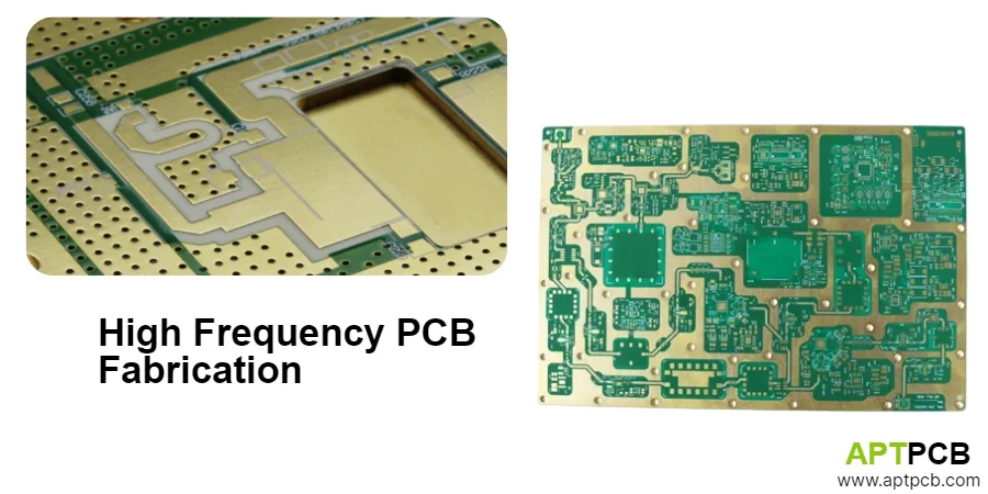
High frequency PCB fabrication encompasses specialized manufacturing processes achieving exceptional precision in dimensions, material properties, and surface characteristics required for RF and microwave circuit performance. These processes must maintain tight tolerances throughout imaging, etching, lamination, drilling, and plating operations that together determine transmission line impedance, insertion loss, and overall electrical performance from megahertz through millimeter-wave frequencies.
At APTPCB, we fabricate high frequency PCBs with specialized processes implementing material-specific parameters, precision equipment, and rigorous process control. Our capabilities support RF high frequency PCB requirements from prototype development through volume production with validated fabrication processes ensuring consistent quality.
Implementing Material Preparation Excellence
High frequency PCB fabrication begins with thorough incoming material verification and conditioning preparing substrates for subsequent processing steps. Proper material handling prevents contamination and damage affecting fabrication quality while conditioning ensures consistent processing results. Inadequate material preparation causes contamination affecting imaging and plating adhesion, moisture-related delamination during lamination, or property variations impacting electrical performance — directly affecting fabrication yield and product quality.
At APTPCB, our material preparation implements systematic procedures ensuring consistent starting conditions.
Key Material Preparation Practices
- Incoming Inspection: Verification of laminate thickness tolerance, surface quality, and material identification with certificate review confirming compliance with specifications for low-loss high frequency PCB materials.
- Material Conditioning: Baking procedures removing absorbed moisture from PTFE and hydrocarbon substrates with material-specific time and temperature parameters preventing lamination issues.
- Surface Treatment: Plasma or chemical treatment enhancing PTFE surface adhesion preparing for photoresist application and subsequent bonding operations.
- Controlled Storage: Temperature and humidity controlled storage areas preventing moisture absorption and maintaining material properties between operations.
- Panel Preparation: Sizing, edge preparation, and tooling hole patterns establishing registration references for subsequent operations with identification marking enabling traceability.
- Cleanroom Handling: Clean glove handling and protective packaging preventing fingerprint contamination on laminate surfaces throughout preparation.
Material Quality Assurance
Through systematic material preparation, controlled handling procedures, and proper conditioning supported by incoming inspection, APTPCB ensures high frequency substrates enter fabrication in optimal condition supporting consistent processing results.
Achieving Precision Innerlayer Fabrication
Innerlayer fabrication for high frequency PCBs requires exceptional precision in photoresist application, imaging, and etching establishing the conductor patterns determining RF circuit performance. Trace width accuracy directly impacts characteristic impedance requiring tight process control throughout innerlayer operations. Inadequate innerlayer precision causes impedance variations degrading return loss, pattern defects creating opens or shorts, or dimensional errors affecting circuit function — directly impacting electrical performance and fabrication yield.
At APTPCB, our innerlayer fabrication implements precision processes achieving demanding tolerances.
Key Innerlayer Fabrication Processes
- Photoresist Application: Dry film lamination achieving uniform thickness across panel surfaces with edge sealing preventing developer penetration and coating parameters optimized for material type.
- Direct Imaging: Laser direct imaging systems achieving ±10μm accuracy eliminating film-related registration errors critical for controlled impedance high frequency PCB fabrication with fine-line geometries.
- Exposure Optimization: Energy optimization balancing resolution against process latitude with environmental controls maintaining dimensional stability during imaging operations.
- Precision Etching: Chemical etch processes with controlled etch factor achieving trace width tolerances to ±0.5 mil with different chemistries optimized for various high frequency materials.
- Etch Factor Characterization: Process monitoring establishing etch compensation factors for each material and copper weight combination enabling accurate line width prediction.
- Automated Optical Inspection: High-resolution AOI detecting opens, shorts, and dimensional violations with measurement data supporting statistical process control.
Innerlayer Quality Verification
By implementing precision imaging, controlled etching, and comprehensive inspection coordinated with statistical process control, APTPCB achieves innerlayer quality supporting demanding high frequency multilayer PCB impedance and performance requirements.
Mastering Specialized Lamination Processes
Lamination of high frequency PCBs requires modified press cycles accounting for the unique thermal characteristics and flow properties of PTFE, hydrocarbon, and ceramic-filled materials. Press parameters including temperature profiles, pressure application, and dwell times must be optimized for each material system. Inadequate lamination causes delamination affecting reliability, dielectric thickness variations impacting impedance control, or void formation degrading electrical performance — significantly affecting product quality and long-term reliability.
At APTPCB, our lamination processes implement material-specific parameters ensuring consistent results.
Key Lamination Capabilities
- PTFE Press Cycles: Extended dwell times and controlled heating rates accommodating PTFE material characteristics with vacuum evacuation removing entrapped air before pressure application.
- Temperature Uniformity: Press platen uniformity within ±2°C ensuring consistent dielectric properties across panel area with monitoring systems recording actual cycle parameters.
- Prepreg Selection: Material-specific prepreg with appropriate flow characteristics and electrical properties compatible with microwave RF PCB performance requirements.
- Registration Systems: Precision tooling maintaining layer alignment through lamination with tolerances supporting multilayer impedance control requirements.
- Sequential Lamination: Multi-stage build processes for complex constructions requiring blind/buried vias or cavity structures with process documentation for each sequential build.
- Post-Lamination Inspection: Dimensional verification confirming panel meets thickness specifications with warpage measurement and surface quality examination.
Lamination Process Assurance
Through material-optimized press cycles, precision registration, and comprehensive process monitoring supported by post-lamination verification, APTPCB achieves consistent lamination quality across diverse high frequency material systems.
Executing Precision Drilling Operations
Drilling high frequency materials presents unique challenges requiring modified parameters addressing PTFE smearing, ceramic filler abrasion, and material softness affecting hole quality. Through-hole drilling, controlled-depth operations, and laser microvia formation each require specialized approaches. Inadequate drilling causes poor hole wall quality affecting plating adhesion, via reliability issues from smear or damage, or stub resonances degrading high frequency performance — directly impacting product reliability and electrical performance.
At APTPCB, our drilling operations implement material-specific processes ensuring hole quality.
Key Drilling Capabilities
- PTFE Drilling Parameters: Optimized spindle speeds, feed rates, and chip loads minimizing smear and heat generation with entry/exit materials selected for PTFE compatibility.
- Ceramic-Filled Material Processing: Carbide drills with specialized geometries and coatings managing accelerated wear from ceramic fillers with tool monitoring ensuring consistent quality.
- Controlled Depth Drilling: CNC systems with ±50μm depth accuracy enabling backdrilling to remove via stubs for RF high frequency PCB applications requiring minimal stub length.
- Laser Microvia Formation: CO2 and UV laser drilling achieving diameters to 75μm for high-density interconnect structures with material-optimized parameters.
- Hole Quality Inspection: Automated inspection of hole diameter, position, and wall quality with cross-section verification validating drilling process performance.
- Desmear Processing: Plasma or chemical desmear removing resin smear from hole walls preparing surfaces for electroless copper deposition compatible with various substrate materials.
Drilling Quality Assurance
By implementing material-optimized drilling parameters, precision depth control, and comprehensive hole quality verification, APTPCB achieves drilling performance supporting demanding high frequency via and interconnect requirements.
Maintaining Metallization Process Control
Plating processes for high frequency PCBs must achieve tight thickness uniformity directly affecting impedance control and via reliability. Electroless copper deposition, electrolytic plating, and surface finish application each require careful process control. Inadequate plating causes impedance variations from thickness non-uniformity, via reliability issues from inadequate hole coverage, or RF performance degradation from inappropriate surface finishes — significantly impacting electrical performance and product reliability.
At APTPCB, our metallization processes implement precision control ensuring consistent performance.
Key Metallization Capabilities
- Electroless Copper Deposition: Uniform conductive layer in drilled holes with void detection ensuring complete coverage before electrolytic plating and process monitoring maintaining bath performance.
- Electrolytic Copper Plating: Pulse reverse plating achieving ±10% thickness uniformity across panel surfaces with current density optimization for hole-to-surface distribution.
- Throwing Power Optimization: Plating parameters achieving adequate thickness in high aspect ratio holes through high frequency PCB manufacturer process expertise.
- XRF Thickness Measurement: In-process monitoring tracking plating thickness at multiple panel positions with statistical analysis supporting process control.
- Surface Finish Selection: ENIG, immersion silver, or OSP application considering RF performance impact, assembly requirements, and reliability through high frequency PCB assembly compatibility.
- Smooth Copper Options: Rolled annealed or reverse-treated copper foils minimizing surface roughness impact on conductor losses at higher frequencies.
Metallization Quality Verification
Through precision plating control, comprehensive thickness monitoring, and appropriate surface finish selection coordinated with application requirements, APTPCB achieves metallization quality supporting demanding impedance control and RF performance specifications.
Ensuring Outer Layer Processing Precision
Outer layer processing defines the final circuit patterns interfacing with components and connectors requiring precision matching innerlayer quality. Imaging, etching, and soldermask application must maintain dimensional accuracy while providing reliable assembly surfaces. Inadequate outer layer processing causes impedance errors from trace width variation, soldermask adhesion issues on PTFE surfaces, or surface quality problems affecting assembly — directly impacting product functionality and reliability.
At APTPCB, our outer layer processing achieves precision matching fabrication requirements.
Key Outer Layer Processes
- Pattern Imaging: Photoresist application on plated surfaces with imaging registration to innerlayer patterns achieving alignment requirements for complex high frequency multilayer PCB designs.
- Precision Etching: Controlled etching maintaining trace widths for impedance control with differential etching protecting circuit patterns while removing background copper.
- Soldermask Application: Liquid photoimageable soldermask with surface preparation addressing PTFE adhesion challenges through plasma treatment or primer application.
- Soldermask Opening Accuracy: Imaging and development achieving registration to underlying pads with tolerances supporting fine-pitch component assembly.
- Legend Printing: Component designators and markings applied without affecting RF performance or assembly processes.
- Surface Treatment: Final cleaning removing contamination before shipping with appropriate packaging protecting board quality.
Outer Layer Excellence
By implementing precision outer layer imaging, controlled etching, and appropriate soldermask processing coordinated with material-specific requirements, APTPCB achieves outer layer quality completing high frequency PCB fabrication to demanding specifications.
Implementing Comprehensive Quality Control
High frequency PCB fabrication quality depends on statistical process control monitoring critical parameters throughout manufacturing. Impedance verification, dimensional inspection, and traceability systems ensure consistent product quality meeting specifications. Inadequate quality control allows process drift causing specification violations, misses defects escaping to customers, or lacks documentation supporting quality investigations — significantly impacting product reliability and customer confidence.
At APTPCB, our quality control implements systematic monitoring ensuring fabrication excellence.
Key Quality Control Practices
- Statistical Process Control: Control charts tracking line width, dielectric thickness, and plating uniformity with capability studies verifying processes meet design requirements through testing quality standards.
- Impedance Verification: TDR testing of production coupons confirming achieved impedance values with statistical analysis relating coupon data to product performance.
- Dimensional Inspection: Coordinate measuring machine verification of critical features including board outline, hole positions, and registration with documentation meeting customer requirements.
- Cross-Section Analysis: Microsection evaluation of layer registration, plating quality, and via structures following standardized IPC procedures with photographic documentation.
- Electrical Testing: Continuity and isolation verification ensuring basic circuit integrity with flying probe or bed-of-nails testing detecting opens and shorts.
- Material Traceability: Complete documentation linking finished products to raw materials, process parameters, and inspection results supporting quality system requirements.
Quality Excellence
Through comprehensive process monitoring, thorough verification testing, and complete traceability documentation supported by certified quality systems, APTPCB delivers high frequency PCB fabrication quality meeting demanding commercial, aerospace, and defense requirements.