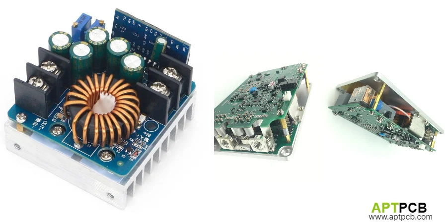
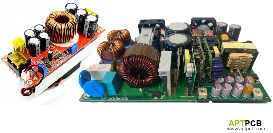
High-power DC-DC converter assemblies handling kilowatts to hundreds of kilowatts require sophisticated power electronics design, advanced thermal management, and precision manufacturing achieving >95% efficiency while operating reliably through millions of switching cycles across telecommunications infrastructure, railway traction systems, industrial automation, renewable energy, and data center applications demanding continuous operation with minimal maintenance over 15-20 year service lives.
At APTPCB, we deliver specialized high-power converter assembly services with high-speed PCB manufacturing expertise implementing advanced topologies including resonant converters, phase-shifted full-bridge designs, and multi-level architectures. Our capabilities span 1kW through 500kW+ converters across voltage ranges from 48V telecom through 1500V+ railway and renewable energy systems with comprehensive validation testing.
Achieving High-Efficiency Power Conversion
Power conversion efficiency directly impacts system economics, thermal management requirements, and environmental sustainability. Each percentage point of efficiency loss translates to kilowatts of heat dissipation requiring expensive cooling infrastructure, wasted energy increasing operating costs, and reduced system reliability from elevated component temperatures. Modern high-power converters target >96% efficiency at rated load with >94% efficiency maintained across 20-100% load ranges.
At APTPCB, our assembly services implement efficiency optimization strategies through topology selection, component specification, and precision manufacturing.
Key Efficiency Optimization Techniques
Advanced Topology Implementation
- Phase-shifted full-bridge (PSFB) converters achieving zero-voltage switching (ZVS) minimizing MOSFET turn-on losses at high switching frequencies (50-200kHz) with high-frequency PCB design
- LLC resonant converters operating at resonant frequency eliminating hard switching losses, achieving >97% peak efficiency through soft-switching of primary and secondary semiconductors
- Multi-level topologies (3-level, 5-level NPC or flying capacitor) reducing dv/dt stress on switches, enabling use of lower-voltage rated devices with superior Rds(on) or Vce(sat) characteristics
- Interleaved parallel converters distributing power across multiple phases reducing current stress per device, improving thermal distribution, and enabling higher aggregate power levels
- Synchronous rectification replacing output diodes with actively-driven MOSFETs eliminating forward voltage drops improving efficiency 2-4% particularly at low output voltages
- Digital control implementation enabling adaptive switching frequency, dynamic dead-time optimization, and predictive control algorithms maximizing efficiency across varying load conditions
Power Semiconductor Selection
- Silicon carbide (SiC) MOSFETs and diodes operating at 150-200°C junction temperatures enabling higher power density, reduced cooling requirements, and efficiency gains from lower switching losses
- Low Rds(on) silicon MOSFETs in synchronous rectification stages minimizing conduction losses dominating at heavy loads
- Fast-recovery diodes or Schottky barriers in auxiliary circuits minimizing reverse recovery losses
- Optimized gate drive design controlling di/dt and dv/dt during switching transitions balancing switching speed against EMI generation and voltage overshoot
- Thermal interface materials (TIM) ensuring minimal thermal resistance between semiconductor packages and heat sinks maintaining junction temperatures within safe operating limits
- PCB stack-up design with controlled impedance minimizing parasitic inductance in power loops reducing switching losses and voltage overshoots
Magnetics Optimization
- Custom transformer designs using high-frequency ferrite cores (3F3, N87, N97) or nanocrystalline materials achieving low core losses at 50-200kHz switching frequencies
- Optimized winding techniques (interleaving, Litz wire, foil windings) minimizing proximity effect losses and AC resistance degrading efficiency at high frequencies
- Integrated magnetic structures combining transformer and filter inductors sharing common cores reducing component count, board area, and losses
- Thermal management of magnetics using potting compounds, heat sinks, or forced air cooling maintaining core temperatures <100°C preventing excessive losses or saturation
- Parasitic capacitance minimization through winding arrangement and shielding reducing common-mode noise and EMI while maintaining high efficiency
- Manufacturing validation through impedance measurement, leakage inductance characterization, and efficiency testing across load ranges
PCB Layout and Material Selection
- Advanced PCB manufacturing with heavy copper layers (4-6oz) in power distribution paths minimizing resistive losses in high-current DC buses
- Minimized parasitic inductance through optimal component placement keeping switching loops compact reducing ringing, overshoot, and switching losses
- High thermal conductivity materials improving heat spreading from power components to heat sinks or ambient air
- Multi-layer construction enabling proper power and ground plane distribution, controlled impedance signal routing, and effective thermal management
- Low-loss dielectric materials (Rogers, Isola) in RF sections and high-frequency switching areas minimizing dielectric losses
- Thermal via arrays beneath power semiconductors, capacitors, and magnetic components transferring heat through PCB layers to thermal management systems
Control and Drive Optimization
- Soft-start and pre-charge circuits limiting inrush currents during startup reducing stress on input capacitors and source impedance
- Adaptive dead-time control eliminating body diode conduction periods minimizing losses during MOSFET transitions
- Valley switching or critical conduction mode operation in resonant converters ensuring switching occurs at voltage minima reducing turn-on losses
- Load-dependent frequency scaling reducing switching frequency at light loads where switching losses dominate maintaining high efficiency across full load range
- Temperature-compensated control adjusting operating parameters maintaining optimal efficiency despite thermal variations in components
- Efficiency telemetry and monitoring enabling predictive maintenance and operational optimization in deployed systems
Validated High-Efficiency Performance
Through advanced topology implementation, optimal component selection, and precision manufacturing processes coordinated through our industrial control expertise, APTPCB delivers high-power converter assemblies achieving industry-leading efficiency targets supporting sustainable, cost-effective power conversion across demanding industrial applications.
Managing Thermal Challenges in Kilowatt Systems
High-power converters dissipate hundreds to thousands of watts as heat requiring comprehensive thermal management preventing semiconductor junction temperatures exceeding specifications (typically 125-150°C), maintaining electrolytic capacitor temperatures below ratings (typically 85-105°C), and controlling ambient temperatures within equipment enclosures. Inadequate thermal design causes immediate failures from thermal shutdown, accelerated aging reducing mean time between failures (MTBF), or catastrophic destruction from thermal runaway.
APTPCB implements multi-faceted thermal strategies ensuring reliable continuous operation at rated power.
Key Thermal Management Strategies
Semiconductor Thermal Interface
- Precision heat sink mounting with controlled torque application ensuring uniform pressure distribution and minimal thermal interface resistance
- Thermal interface materials selection (thermal grease, phase-change materials, graphite pads) achieving <0.5°C/W thermal resistance between semiconductor packages and heat sinks
- Direct copper bonding or insulated metal substrates (IMS) for highest-power semiconductors eliminating PCB thermal resistance bottleneck
- Package selection prioritizing exposed pad designs (D2PAK, TO-247 with back drain, PowerPAK) maximizing heat extraction from die to external cooling
- Parallel device mounting distributing power dissipation across multiple semiconductors reducing peak temperatures and thermal stress
- High thermal PCB materials with enhanced thermal conductivity (2-5W/mK vs. standard FR4 at 0.3W/mK) improving lateral heat spreading
Heat Sink Design and Integration
- Extruded aluminum heat sinks with optimized fin geometry balancing thermal performance, airflow resistance, and cost
- Heat pipe integration enabling heat transfer from concentrated sources to large surface area sinks achieving superior thermal performance in compact designs
- Liquid cooling systems using cold plates, microchannel heat exchangers, or immersion cooling for highest power densities (>500W/in³) where air cooling insufficient
- Thermal simulation (CFD analysis) predicting temperature distributions, optimizing airflow paths, and validating thermal design before prototype builds
- Heat sink surface treatments (anodizing, black coating) improving radiative heat transfer particularly important in natural convection applications
- Mounting interface design minimizing mechanical stress from CTE mismatch between PCB, heat sinks, and semiconductors preventing solder joint fatigue
Airflow Management
- Forced air cooling with axial or centrifugal fans sized for required airflow at acceptable noise levels and power consumption
- Plenum design directing airflow through heat sink fins maximizing convective heat transfer while minimizing bypass flow
- Filter integration preventing dust accumulation degrading thermal performance while maintaining adequate airflow
- Redundant fan configurations ensuring continued operation despite single fan failure critical for high-availability applications
- Variable speed control adjusting fan speed based on temperature feedback minimizing noise and power consumption at reduced loads
- Thermal zone separation isolating high-heat-dissipating sections preventing thermal coupling to temperature-sensitive analog circuits or control electronics
Component Thermal Management
- Metal core PCB or aluminum substrates in power stage areas providing superior heat spreading compared to FR4
- Capacitor selection prioritizing high-ripple-current, high-temperature ratings (105°C or 125°C electrolytic capacitors) surviving elevated ambient temperatures
- Thermal via arrays (50-100 vias per component) transferring heat from surface-mount power components through PCB to opposite-side cooling
- Component placement maintaining adequate spacing between heat-generating devices preventing localized hot spots from thermal coupling
- Thermal cameras and embedded sensors during validation testing identifying hot spots requiring design iteration or enhanced cooling
- Manufacturing process controls ensuring consistent thermal interface material application and heat sink mounting achieving repeatable thermal performance
Environmental Considerations
- Altitude derating accounting for reduced air density affecting convective cooling efficiency at high elevations (data centers, mountain telecommunications)
- Humidity management preventing condensation on electronics in tropical environments or preventing excessive drying in arid climates
- Temperature cycling qualification validating mechanical integrity and thermal performance through -40°C to +85°C ambient temperature ranges
- Thermal shock testing ensuring solder joints and component attachments survive rapid temperature changes during power cycling
- Long-term reliability prediction using thermal models and accelerated life testing estimating MTBF under various operating conditions
- Field failure analysis identifying thermal-related failures implementing design improvements preventing recurrence
Thermally Robust Design Implementation
By integrating comprehensive thermal analysis, validated heat sink designs, and proper material selection supported by our PCB quality manufacturing standards, APTPCB enables high-power converter assemblies maintaining safe operating temperatures throughout extended service lives supporting reliable telecommunications, industrial, and transportation applications.
Implementing Advanced Control Topologies
High-power converter control systems coordinate switching timing, regulate output voltage and current, implement protection functions, and provide diagnostic capabilities requiring sophisticated analog and digital circuitry. Modern converters employ digital control using DSPs, FPGAs, or microcontrollers enabling advanced algorithms, adaptive operation, and communication interfaces while maintaining microsecond-level control loop response times critical for stability and transient performance.
APTPCB assembles complex control boards integrating high-speed digital processing with precision analog sensing.
Key Control Implementation Requirements
Digital Control Platform Integration
- High-performance DSP or FPGA implementation executing control algorithms at >100kHz update rates maintaining stability and fast transient response
- Multiple high-resolution PWM outputs (12-16 bit) driving parallel phases, interleaved converters, or multi-level topologies with nanosecond timing precision
- High-speed ADC interfaces (12-16 bit at 1-10MSPS) digitizing output voltage, current, and temperature measurements for control loop feedback
- Communication interfaces (CAN, Ethernet, RS-485) enabling remote monitoring, configuration, and integration into supervisory control systems
- Non-volatile memory storage for calibration parameters, configuration settings, and operational data logging
- Firmware update capability through communication interfaces enabling field upgrades adding features or fixing bugs without hardware replacement
Precision Analog Sensing
- Output voltage sensing with <0.1% accuracy across full voltage range enabling tight regulation required by sensitive loads
- Output current sensing using Hall effect sensors, current transformers, or shunt resistors measuring DC, AC, or pulsating currents in converter output stages
- Input voltage and current monitoring providing power measurement, efficiency calculation, and source protection functions
- Temperature measurement using thermistors, thermocouples, or integrated sensors monitoring semiconductors, magnetics, and ambient conditions
- Isolation amplifiers maintaining safety barriers between high-voltage power stages and low-voltage control electronics
- PCB fabrication process controls ensuring signal integrity through proper grounding, shielding, and noise filtering
Control Algorithm Implementation
- Voltage mode control with compensated error amplifiers achieving specified transient response and stability margins across operating ranges
- Current mode control improving dynamic response and providing inherent current limiting for overcurrent protection
- Predictive or model-based control calculating optimal switching patterns based on system state and load predictions
- Soft-start algorithms gradually ramping output voltage preventing inrush currents and voltage overshoots potentially damaging loads
- Active current sharing in parallel converters distributing load current evenly preventing unbalanced loading causing premature failure
- Synchronization and phase management in multi-converter systems minimizing input/output ripple and optimizing efficiency
Protection and Diagnostic Features
- Overvoltage and undervoltage protection comparing output against limits immediately shutting down converter preventing load damage
- Overcurrent protection with foldback limiting reducing output during overload preventing thermal damage while maintaining partial functionality
- Overtemperature protection monitoring multiple thermal sensors implementing graduated responses from derating through shutdown
- Short circuit protection detecting output shorts within microseconds opening output to prevent semiconductor destruction
- Input protection monitoring source voltage and current protecting against reverse polarity, overvoltage transients, or supply failures
- Fault logging and diagnostic reporting storing fault conditions, environmental data, and operational parameters supporting field troubleshooting
Communication and Monitoring
- PMBus or proprietary communication protocols providing real-time telemetry (voltage, current, temperature, efficiency, warnings)
- Configuration interfaces enabling remote adjustment of output voltage, current limits, switching frequency, and protection thresholds
- Alarm outputs (relay, open-collector, or digital signals) providing immediate notification to supervisory systems during fault conditions
- Power management interfaces coordinating multiple converters in redundant configurations supporting high-availability applications
- Firmware version reporting and bootloader functionality enabling remote software updates maintaining system security and functionality
- Data logging recording operational parameters supporting predictive maintenance and optimization
Advanced Control Capabilities
Through sophisticated digital control implementation, precision analog measurement, and comprehensive protection functions validated through PCB surface finishes ensuring reliable signal connections, APTPCB delivers high-power converters with intelligent control systems meeting demanding telecommunications, data center, and industrial automation requirements.
Optimizing Magnetics Integration
Magnetic components (transformers, inductors) represent critical elements in high-power converters accounting for 20-40% of total losses, determining power density and converter size, and influencing EMI performance. Optimal magnetics design requires balancing core losses, winding losses, leakage inductance, and physical size while maintaining proper insulation, thermal management, and manufacturing feasibility.
APTPCB coordinates magnetics design and integration ensuring performance, manufacturability, and cost-effectiveness.
Key Magnetics Design Considerations
Core Material and Geometry Selection
- Ferrite materials (3F3, N87, N97) for high-frequency operation (50-300kHz) offering low core losses and adequate saturation flux density
- Powder cores (iron powder, sendust, MPP) for filter inductors requiring high DC bias capability without significant inductance drop
- Nanocrystalline cores for highest efficiency demanding applications offering ultra-low losses but at premium cost
- Core geometry optimization (ETD, EE, pot cores, toroids) balancing winding window area, surface area for cooling, and magnetic path length
- Airgap selection and positioning controlling inductance value while managing fringing flux and hot-spot formation
- Temperature rating ensuring core Curie temperature and loss characteristics remain stable across full operating temperature range
Winding Design and Optimization
- Litz wire construction for high-frequency windings eliminating skin effect and proximity effect losses maintaining low AC resistance
- Copper foil windings for high-current, lower-frequency applications minimizing DC resistance while providing excellent thermal performance
- Interleaving primary and secondary windings reducing leakage inductance critical for ZVS operation and minimizing voltage ringing
- Layer insulation selection (polyimide tape, Nomex paper, epoxy impregnation) providing required dielectric strength meeting safety standards
- Winding arrangement minimizing interwinding capacitance reducing common-mode noise and EMI while maintaining safety barriers
- Termination methods (PCB-mount, flying leads, threaded terminals) optimized for manufacturability, current capacity, and thermal management
Thermal Design Integration
- Core loss calculation at operating frequency and flux density determining heat generation requiring dissipation
- Winding loss calculation including DC resistance and AC effects predicting thermal rise and hot-spot temperatures
- Thermal modeling or measurement validating core and winding temperatures remain below material limits (typically 100-130°C)
- Bobbin material selection prioritizing high-temperature plastics (PPS, LCP) withstanding soldering temperatures and operating conditions
- Potting or encapsulation using thermally conductive materials improving heat transfer to ambient while providing mechanical support
- Heat sink integration or forced air cooling for highest power designs where natural convection insufficient
Manufacturing and Quality Control
- Automated winding equipment ensuring consistent turn counts, layer arrangement, and winding tension
- Insulation testing (hipot, partial discharge) validating dielectric strength between windings and from windings to core
- Inductance and leakage inductance measurement confirming magnetic parameters meet specifications
- Core loss measurement at operating frequency validating material properties and identifying manufacturing defects
- Assembly documentation with turn counts, wire specifications, and construction photos supporting troubleshooting and reproduction
- Qualification testing including thermal cycling, vibration, and life testing validating long-term reliability
PCB Integration Considerations
- Footprint design accommodating magnetic component dimensions while maintaining adequate clearance to adjacent components and enclosure walls
- Pin assignment optimizing PCB routing minimizing trace lengths and layer transitions in high-current paths
- Mounting method (through-hole, surface-mount, pressure contact) balancing mechanical robustness and manufacturing efficiency
- EMI shielding integration if required using copper tape, ferrite shields, or aluminum enclosures reducing radiated emissions
- Thermal coupling design enabling heat transfer from magnetic component to PCB, heat sink, or ambient air
- Keep-out areas around magnetics preventing placement of temperature-sensitive components affected by magnetic component heating
Optimized Magnetic Performance
By implementing comprehensive magnetics design, coordinating with specialized suppliers, and validating performance through testing programs, APTPCB ensures high-power converter magnetic components achieve efficiency targets while meeting size, cost, and manufacturability requirements supporting successful industrial and telecommunications products.
Ensuring EMC Compliance
High-power converters generate substantial electromagnetic interference (EMI) from high di/dt and dv/dt switching transients requiring comprehensive EMC design strategies achieving compliance with conducted emissions (EN 55022, FCC Part 15), radiated emissions, and immunity requirements. Non-compliant designs cause interference with adjacent equipment, fail regulatory testing requiring expensive redesign, or experience operational disruptions from external interference in industrial or electromagnetic-hostile environments.
APTPCB implements EMC best practices throughout design and manufacturing ensuring compliance and reliable operation.
Key EMC Design Requirements
Conducted Emissions Management
- Input filter design using common-mode and differential-mode filtering reducing conducted noise on power lines to levels required by EN 55022 Class A/B or FCC Part 15 limits
- Common-mode choke design with adequate magnetizing inductance and parasitic capacitance control providing high-frequency noise attenuation
- X and Y capacitor selection balancing noise attenuation against inrush current, leakage current, and safety requirements
- Filter component layout minimizing parasitic inductance and ensuring proper grounding preventing filter effectiveness degradation
- Shielding and grounding strategies preventing EMI bypass around input filters through parasitic coupling paths
- Validation testing using LISN and spectrum analyzer during development identifying non-compliance issues before formal testing
Radiated Emissions Control
- PCB layout following low-EMI design guidelines minimizing loop areas in high di/dt paths reducing magnetic field generation
- Switching edge rate control using gate resistors or active gate drive techniques slowing transitions reducing high-frequency spectral content
- Shielding enclosures using conductive gaskets, filtered connectors, and proper grounding maintaining electromagnetic barrier integrity
- Cable management using shielded cables, ferrite beads, or proper twisted-pair routing minimizing antenna effects from interconnect wiring
- Common-mode current minimization through balanced layout, Y-capacitor placement, and proper transformer design reducing antenna mode radiation
- Pre-compliance testing in semi-anechoic chambers during development identifying and resolving emissions issues before formal compliance testing
Immunity Requirements
- ESD protection using TVS diodes, gas discharge tubes, or polymer suppressors on external interfaces preventing damage from electrostatic discharge
- Transient immunity design withstanding fast transients (EFT/burst per IEC 61000-4-4) common in industrial environments with inductive loads
- Surge immunity protecting against lightning-induced surges (IEC 61000-4-5) on power and communication interfaces in exposed installations
- RF immunity ensuring operation continues without disruption despite strong RF fields (IEC 61000-4-3) from nearby transmitters or industrial equipment
- Conducted disturbance immunity maintaining operation despite voltage dips, interruptions, or harmonics on power supply (IEC 61000-4-11, -13, -17)
- Proper grounding preventing ground loops, noise injection, or safety hazards while maintaining EMC performance
PCB Layout Best Practices
- Solid ground and power planes providing low-impedance return paths and reducing loop areas minimizing emissions
- Component placement separating noisy sections (switching power stage) from sensitive circuits (control, sensing) through physical spacing and grounding
- Critical signal routing using microstrip or stripline with controlled impedance maintaining signal integrity and reducing radiation
- Via placement and density optimizing return current paths and minimizing stub antennas contributing to radiated emissions
- Filtering and decoupling at board interfaces preventing EMI ingress or egress through power and signal connections
- Design rule checking validating clearances, creepage distances, and isolation barriers maintaining safety while supporting EMC
Compliance Testing and Validation
- Pre-compliance testing during development using near-field probes, current probes, and spectrum analyzers identifying problem areas
- Test setup optimization minimizing facility-related issues ensuring representative measurements and avoiding test failures from setup artifacts
- Formal compliance testing at accredited laboratories generating test reports required for product certifications and market access
- International standards compliance supporting global sales including CE marking (Europe), FCC (US), CCC (China), and other regional requirements
- Manufacturer's Declaration of Conformity documentation supported by test reports, technical files, and risk assessments
- Post-market surveillance maintaining compliance despite design changes, component obsolescence, or new regulatory requirements
EMC Compliant Implementation
By integrating EMC considerations throughout design, implementing proven filtering and shielding strategies, and conducting thorough validation testing, APTPCB delivers high-power converters achieving regulatory compliance supporting global market access and reliable operation in electromagnetically challenging industrial environments.
Supporting Diverse Industrial Applications
High-power DC-DC converters serve diverse applications spanning telecommunications (48V infrastructure, 5G base stations), railway traction (600-3000V auxiliary power), industrial automation (motor drives, PLCs, robotics), renewable energy (solar MPPT, energy storage), and data centers (48V direct distribution) requiring application-specific optimizations in voltage range, transient response, protection features, and environmental specifications.
APTPCB provides flexible manufacturing supporting diverse application requirements through configurable designs and scalable production.
Key Application Support Capabilities
Telecommunications Infrastructure
- 48V nominal input converters (36-75V operating range) matching telecom industry standards with holdup time requirements supporting brief power interruptions
- Output voltage options (5V, 12V, 24V, 48V) powering diverse equipment including baseband processors, RF amplifiers, and site equipment
- High reliability and availability targeting >99.999% uptime through redundant configurations, active current sharing, and hot-swap capability
- Compact 19" rack-mount configurations maximizing power density in space-constrained equipment rooms and outdoor cabinets
- Operating temperature range (-40°C to +65°C) surviving harsh outdoor environments and unconditioned equipment shelters
- Network management integration (SNMP, PMBus) enabling remote monitoring and control within telecommunications management systems
Railway and Transportation
- Wide input voltage range (400-1000VDC or 1500-3000VDC) accommodating variations from regenerative braking, catenary voltage drops, or multi-system operation
- Ruggedized construction withstanding vibration (IEC 61373), shock, and harsh environmental conditions typical in railway applications
- Safety certifications (EN 50155, IRIS) meeting railway industry requirements for electronic equipment in rolling stock
- Galvanic isolation (4-6kV) ensuring passenger safety separating high-voltage traction systems from low-voltage auxiliary equipment
- Transient immunity handling inductive load switching, pantograph arcing, and traction motor commutation without operational disruption
- Long service life (30+ years) matching railway vehicle lifespans with proven reliability and maintainability
Industrial Automation and Process Control
- Universal input (85-265VAC or 100-800VDC) accommodating diverse industrial power standards globally without modification
- Regulated outputs powering PLCs, distributed I/O, motor drives, sensors, and actuators with tight tolerance (<±1%) and low ripple
- Industrial protocol support (Modbus, Profinet, EtherCAT) integrating power supply monitoring into factory automation networks
- Harsh environment ratings (IP65, C3/C4 corrosion resistance) surviving factory floor conditions with dust, humidity, chemicals, and temperature extremes
- SIL ratings (SIL 2/3) supporting functional safety requirements in process industries and automated machinery
- Flexible mounting (DIN rail, panel mount, chassis mount) accommodating various industrial enclosure designs
Renewable Energy and Storage
- MPPT algorithm support extracting maximum power from solar panels across varying irradiance and temperature conditions
- Wide voltage range (200-1000VDC input) accommodating high-voltage solar strings and battery banks in utility-scale installations
- Bidirectional operation supporting battery charging and discharging in energy storage systems
- Grid-tie synchronization integrating renewable generation with utility power maintaining power quality and grid codes compliance
- Environmental certifications (IEC 62109, UL 1741) meeting photovoltaic and energy storage safety standards
- Outdoor ratings (NEMA 3R/4) with conformal coating and environmental protection surviving 25+ year solar installation lifetimes
Data Center Power Distribution
- 380V or 48V direct distribution reducing conversion stages improving overall data center efficiency (PUE)
- High power density (>20W/in³) minimizing rack space consumption maximizing server density in data centers
- Hot-swap and redundant configurations (N+1, 2N) ensuring continuous operation despite converter failures in mission-critical installations
- Digital management (PMBus, I²C) monitoring efficiency, temperatures, and status integrating into data center infrastructure management (DCIM) systems
- Efficiency optimization (96-98%) reducing cooling requirements and operating costs critical in large-scale data centers
- Scalable architectures supporting distributed power architectures with intermediate bus voltages (12V, 48V) optimizing point-of-load regulation
Application-Optimized Solutions
By understanding diverse application requirements, implementing flexible designs, and providing engineering support throughout development and production, APTPCB enables equipment manufacturers deploying optimized high-power DC-DC converter solutions across telecommunications, transportation, industrial, renewable energy, and data center markets worldwide.