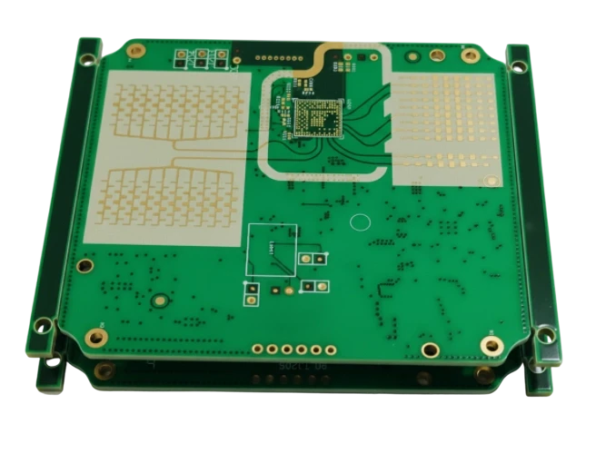
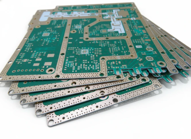
The rapid evolution of 5G networks, automotive radar, and satellite communications has placed the high-speed Beamforming module board at the center of modern RF engineering. Unlike standard printed circuit boards, these modules are active, complex systems responsible for steering wireless signals electronically without moving parts. Achieving the necessary phase accuracy and signal integrity requires a manufacturing partner who understands the physics of high-frequency materials. At APTPCB (APTPCB PCB Factory), we see firsthand how critical precise fabrication is for these advanced modules.
This guide covers the entire lifecycle of a high-speed Beamforming module board, from initial definition and material selection to the final validation steps required for mass production.
Key Takeaways
- Definition: A high-speed Beamforming module board is a specialized PCB integrating antenna arrays and phase-shifting logic to steer RF signals electronically.
- Critical Metric: Phase stability is the most important performance indicator; even minor etching variations can disrupt the beam angle.
- Material Strategy: Hybrid stackups (mixing FR4 with PTFE/Ceramic) are standard to balance cost and RF performance.
- Manufacturing Risk: Layer registration and back-drill depth accuracy are the top causes of yield loss in volume production.
- Validation: Testing must go beyond standard electrical connectivity to include functional RF testing and thermal cycling.
- Assembly: Beamforming module board assembly requires high-precision SMT placement for bare die or flip-chip components to minimize parasitic inductance.
- Misconception: High cost does not always equal high performance; over-specifying materials for digital layers wastes budget without improving RF signal quality.
What “beamforming module board” means (scope & boundaries)
To understand the manufacturing challenges, we must first define the scope. A high-speed Beamforming module board is not merely a carrier for components; it is an integral part of the antenna system. In traditional RF designs, the antenna and the radio logic were often separate. In beamforming modules, they are tightly integrated, often on the same substrate or within a multi-board sandwich structure.
The Core Functionality
Beamforming works by manipulating the phase and amplitude of signals emitted from multiple antenna elements. By constructively interfering with the waves, the module "steers" the beam toward a specific user or target. This requires the PCB to maintain exceptional impedance control and phase consistency across all channels.
Types of Architectures
- Analog Beamforming: Phase shifting happens in the RF domain. The PCB must handle high-frequency analog signals with minimal loss.
- Digital Beamforming: Phase shifting happens in the digital baseband. The PCB requires extremely high-speed digital routing (SerDes) alongside the RF front end.
- Hybrid Beamforming: A combination of both, commonly used in 5G mmWave massive MIMO systems. This is the most complex Beamforming module board design to manufacture due to the mix of signal types.
Scope of "High-Speed"
In this context, "high-speed" refers to two distinct aspects:
- RF Frequency: Carrier frequencies ranging from sub-6GHz up to mmWave (24GHz, 77GHz, etc.).
- Data Rate: The digital control interfaces (JESD204B/C, Ethernet) running at multi-gigabit speeds to feed the beamforming ICs.
Metrics that matter (how to evaluate quality)
Building a reliable module requires tracking specific metrics. Standard PCB IPC class requirements are often insufficient for RF applications.
| Metric | Why it matters | Typical Range / Factors | How to Measure |
|---|---|---|---|
| Phase Stability | Variations in phase shift cause beam squint (aiming errors) and side-lobe generation. | < ±5 degrees across the array. Influenced by Dk homogeneity. | Vector Network Analyzer (VNA) on test coupons. |
| Insertion Loss | High loss reduces range and increases power consumption, generating more heat. | < 0.5 dB/inch (material dependent). Driven by copper roughness and Df. | S-Parameter (S21) measurement. |
| Dk (Dielectric Constant) Tolerance | Variations in Dk change trace impedance and propagation delay, ruining phase accuracy. | ±0.05 or better for high-end RF laminates. | IPC-TM-650 test methods or ring resonators. |
| Copper Surface Roughness | Rough copper increases skin effect losses at high frequencies (mmWave). | VLP (Very Low Profile) or HVLP (< 1µm Rz). | Profilometer or SEM analysis. |
| Layer-to-Layer Registration | Misalignment affects vertical transitions (vias), causing impedance discontinuities. | < 3 mils (75µm) for high-density designs. | X-Ray inspection and micro-sectioning. |
| Thermal Conductivity | Power Amplifiers (PAs) generate immense heat; poor dissipation leads to thermal drift. | > 0.5 W/mK for dielectric; Metal core or coin usage often required. | Thermal imaging under load. |
| Passive Intermodulation (PIM) | Nonlinearities in the PCB (rusty copper, poor solder) create interference. | < -150 dBc (critical for cellular base stations). | PIM tester (IEC 62037). |
How to choose (trade-offs by scenario)
Selecting the right architecture and materials is a balancing act between performance, thermal management, and cost. Below are common scenarios and how to choose the right high-speed Beamforming module board configuration.
Scenario 1: 5G mmWave Base Station (28 GHz / 39 GHz)
- Priority: Signal Integrity and Low Loss.
- Trade-off: High material cost vs. Power efficiency.
- Guidance: Use a Hybrid Stackup. Utilize high-performance PTFE-based materials (like Rogers or Taconic) for the top RF layers and standard high-Tg FR4 for the digital/power layers below. This reduces cost compared to a full PTFE board while maintaining RF performance.
- Key Feature: Requires High Frequency PCB fabrication techniques.
Scenario 2: Automotive Radar (77 GHz)
- Priority: Reliability and Safety.
- Trade-off: Extreme environment durability vs. Miniaturization.
- Guidance: Ceramic-filled hydrocarbon laminates are preferred over pure PTFE due to better dimensional stability and easier processing. The design often uses "Antenna on Package" (AoP) or very short traces to the antenna elements.
- Key Feature: Strict adherence to automotive quality standards (IATF 16949).
Scenario 3: Satellite Communication (LEO Terminals)
- Priority: Phase Accuracy over wide angles.
- Trade-off: Large board size vs. Warpage control.
- Guidance: Large arrays are prone to warping during reflow. Choose materials with matched Coefficient of Thermal Expansion (CTE) to copper. Symmetrical stackups are non-negotiable here to prevent bowing.
- Key Feature: Low outgassing materials are required if the board is for the space segment.
Scenario 4: Sub-6GHz Massive MIMO
- Priority: Thermal Management and Integration Density.
- Trade-off: Heat dissipation vs. Layer count.
- Guidance: These boards carry many active components. A metal-core PCB or embedded copper coins are often necessary to pull heat away from the Power Amplifiers. The dielectric loss is less critical than at mmWave, so mid-loss materials (like Megtron 6) are a good sweet spot.
- Key Feature: HDI PCB technology is essential to route the massive number of digital control lines.
Scenario 5: Portable/Handheld Beamforming Devices
- Priority: Size and Weight (SWaP).
- Trade-off: Integration vs. Isolation.
- Guidance: Rigid-Flex solutions allow the antenna array to be positioned optimally while the logic board sits elsewhere. However, the flex transition must be impedance matched perfectly.
- Key Feature: Flexible liquid crystal polymer (LCP) materials offer excellent high-frequency performance.
Scenario 6: Prototype vs. Mass Production
- Priority: Speed vs. Yield.
- Trade-off: Quick-turn availability vs. Cost optimization.
- Guidance: For prototypes, stick to stocked materials even if they are "over-spec." For mass production, work with APTPCB to qualify a lower-cost equivalent material that meets the specific Dk/Df requirements of your design.
Implementation checkpoints (design to manufacturing)
Moving from a schematic to a physical board requires a rigorous process. Use this checklist to ensure your Beamforming module board design is manufacturable.
1. Stackup Definition and Material Validation
- Recommendation: Define the stackup before routing. Confirm material availability with the fabricator.
- Risk: Designing around a material that has a 20-week lead time or is incompatible with sequential lamination.
- Acceptance: Fabricator-approved stackup drawing with calculated impedance tables.
2. Hybrid Material Compatibility
- Recommendation: When mixing FR4 and high-frequency laminates, ensure their CTE (Z-axis expansion) values are compatible to prevent delamination during reflow.
- Risk: Layer separation during assembly.
- Acceptance: Thermal stress test (solder float) results on test coupons.
3. Trace Width and Impedance Control
- Recommendation: Use geometry that allows for standard etching tolerances. Avoid traces < 3 mils for impedance controlled lines if possible, as etching variations have a larger percentage impact on impedance.
- Risk: High VSWR and signal reflection.
- Acceptance: TDR (Time Domain Reflectometry) testing on production panels.
4. Grounding and Shielding Via Fences
- Recommendation: Place stitching vias (via fences) along RF lines to suppress mode conversion and isolate channels. Spacing should be < λ/8 of the highest frequency.
- Risk: Crosstalk between beamforming channels, degrading beam definition.
- Acceptance: Electromagnetic simulation verification and visual inspection of via integrity.
5. Surface Finish Selection
- Recommendation: Use Immersion Silver or ENEPIG. Avoid HASL (too uneven) and standard ENIG (nickel is magnetic and lossy at high frequencies).
- Risk: Increased insertion loss and passive intermodulation (PIM).
- Acceptance: Surface finish thickness measurement (XRF).
6. Back-Drilling (Controlled Depth Drilling)
- Recommendation: Remove via stubs on high-speed lines. Stubs act as antennas, causing resonance and signal notches.
- Risk: Severe signal degradation at specific resonant frequencies.
- Acceptance: Micro-section analysis to verify stub remainder is within tolerance (usually < 10 mils).
7. Thermal Management Strategy
- Recommendation: Design thermal vias under PA pads. Consider embedded copper coins for high-power modules.
- Risk: Overheating leads to gain compression and phase drift.
- Acceptance: Thermal simulation and prototype thermal profiling.
8. Registration and Scaling Factors
- Recommendation: High-frequency materials scale differently than FR4 during lamination. The fabricator must apply precise scaling factors.
- Risk: Pad-to-drill misalignment, causing breakouts on fine-pitch BGAs.
- Acceptance: X-Ray verification of inner layer registration.
9. Solder Mask Considerations
- Recommendation: Remove solder mask from high-frequency RF traces (solder mask window) or use a specialized low-loss LPI mask. Standard mask adds loss and alters impedance.
- Risk: Unpredictable Dk changes due to mask thickness variation.
- Acceptance: Visual inspection against Gerber files.
10. Panelization for Assembly
- Recommendation: Ensure the panel design supports the rigidity needed for Beamforming module board assembly. Thin RF cores may need a fixture or a thicker waste border.
- Risk: Board warping during SMT reflow.
- Acceptance: Warpage simulation or trial run.
Common mistakes (and the correct approach)
Even experienced engineers can stumble when transitioning to beamforming hardware. Here are common pitfalls.
Mistake 1: Treating the PCB as a passive component
The Error: Assuming the PCB is just a connector. In beamforming, the PCB is the filter, the coupler, and the antenna. The Fix: Simulate the PCB traces and vias in 3D EM software (HFSS/CST) and treat the laminate manufacturing tolerances as part of your error budget.
Mistake 2: Over-specifying tolerances
The Error: Demanding ±2% impedance control when ±5% is sufficient, or requiring Class 3 for non-critical digital layers. The Fix: Focus tight tolerances only on the RF layers. Over-specifying drives up cost and yield loss without adding system value.
Mistake 3: Ignoring Copper Roughness
The Error: Using standard ED (Electro-Deposited) copper for mmWave designs. The Fix: Specify VLP (Very Low Profile) or RA (Rolled Annealed) copper. At 28GHz+, the skin depth is so shallow that current flows through the rough peaks and valleys, significantly increasing resistance and loss.
Mistake 4: Poor Reference Plane Management
The Error: Routing RF traces over splits in the ground plane or changing reference planes without nearby stitching vias. The Fix: Maintain continuous ground reference. If a layer change is needed, place ground vias immediately adjacent to the signal via to provide a return current path.
Mistake 5: Neglecting the "Fiber Weave Effect"
The Error: Running high-speed differential pairs parallel to the glass weave pattern of the laminate. The Fix: Rotate the design 10 degrees on the panel (zigzag routing) or use "spread glass" materials to ensure consistent Dk along the trace length.
Mistake 6: Inadequate DFM Review
The Error: Sending files to production without a specific RF DFM check. The Fix: Engage with APTPCB early. We check for aspect ratios, hybrid lamination risks, and drilling limitations specific to RF materials.
FAQ (cost, lead time, materials, testing)
Q: What is the biggest cost driver for a high-speed Beamforming module board? A: The laminate material is the primary driver. High-frequency PTFE materials can be 5-10x the cost of FR4. The second driver is the layer count and the number of sequential lamination cycles required for HDI structures.
Q: How does lead time compare to standard PCBs? A: Lead times are generally longer (3-5 weeks standard) because high-frequency laminates are often not stocked in every thickness and copper weight combination. Hybrid stackups also require more complex pressing cycles.
Q: Can I use standard FR4 for 5G beamforming boards? A: For sub-6GHz (e.g., 3.5 GHz), high-performance FR4 (like Isola 370HR) might suffice. However, for mmWave (24GHz+), standard FR4 has too much loss and Dk instability. You must use specialized RF materials.
Q: What specific testing should I request for acceptance? A: Beyond standard E-test (Open/Short), request TDR (Impedance) coupons, S-parameter measurements (Insertion Loss) on test structures, and PIM testing if the application is high-power.
Q: How do you handle the "Beamforming module board assembly" of bare dies? A: This requires Wire Bonding or Flip Chip assembly capabilities. The PCB surface finish must be compatible (usually ENEPIG or Soft Gold) and the flatness must be tightly controlled to ensure successful bonding.
Q: What is the acceptance criteria for back-drilling? A: The remaining stub length is the critical criteria. Typically, we aim for a stub length of less than 10 mils (0.25mm). This is verified via micro-sectioning a coupon from the production panel.
Q: Why is "spread glass" recommended for these boards? A: Standard glass weave has gaps (resin-rich areas) and bundles (glass-rich areas). High-speed signals traveling over these variations experience phase jitter. Spread glass minimizes these gaps, providing a homogeneous Dk environment.
Q: How do I specify the stackup for a quote? A: Provide the target frequencies, required impedance values (e.g., 50Ω SE, 100Ω Diff), and preferred material manufacturers. Alternatively, provide the layer count and let the fabricator propose a valid hybrid stackup.
Related pages & tools
To further assist in your design and procurement process, utilize these resources:
- Material Selection: Explore our RF/Microwave Material options to find the right balance of Dk and cost.
- Design Guidelines: Review our DFM Guidelines to ensure your layout is ready for manufacturing.
- Impedance Planning: Use our Impedance Calculator for initial stackup estimation.
- Antenna Specifics: Learn more about Antenna PCB manufacturing capabilities.
Glossary (key terms)
| Term | Definition |
|---|---|
| Phased Array | An antenna array that creates a beam of radio waves which can be electronically steered to point in different directions. |
| MIMO (Multiple Input Multiple Output) | A technology using multiple transmitters and receivers to transfer more data at the same time. |
| Hybrid Stackup | A PCB layer buildup that uses different materials (e.g., FR4 and PTFE) to optimize cost and performance. |
| Dk (Dielectric Constant) | A measure of a material's ability to store electrical energy in an electric field; affects signal speed and impedance. |
| Df (Dissipation Factor) | A measure of the power loss rate of the electrical signal as it passes through the dielectric material. |
| Skin Effect | The tendency of high-frequency alternating current to distribute itself within the conductor so that the current density is largest near the surface. |
| Back-drilling | The process of drilling out the unused portion of a plated through-hole (via stub) to reduce signal reflection. |
| CTE (Coefficient of Thermal Expansion) | The rate at which a material expands with heat. Mismatch between copper and dielectric causes reliability issues. |
| SerDes | Serializer/Deserializer; high-speed communication blocks used to convert parallel data to serial data for transmission. |
| PIM (Passive Intermodulation) | Signal distortion caused by nonlinearities in passive components (like the PCB copper or solder joints). |
| ENEPIG | Electroless Nickel Electroless Palladium Immersion Gold; a universal surface finish good for soldering and wire bonding. |
| Beam Squint | A change in the beam steering angle as a function of frequency, often caused by phase errors in the PCB. |
Conclusion (next steps)
Successfully deploying a high-speed Beamforming module board requires more than just a good schematic; it demands a holistic approach to materials, stackup, and manufacturing tolerances. As frequencies rise and integration densities increase, the margin for error vanishes.
Whether you are prototyping a new radar system or scaling a 5G base station, the key to success lies in early collaboration. By addressing material compatibility, thermal strategies, and DFM checks during the design phase, you avoid costly respins and ensure your product performs as simulated.
Ready to move forward? When requesting a quote or DFM review from APTPCB, please provide:
- Gerber Files: Including all copper layers, drill files, and outline.
- Stackup Requirements: Preferred materials (or electrical requirements if you want us to propose a stackup).
- Impedance Specifications: Target ohms and trace widths.
- Frequency Range: Operating frequency helps us validate material choices.
- Special Requirements: Back-drilling, edge plating, or specific surface roughness needs.
Contact our engineering team today to ensure your beamforming project is built for speed and reliability.