Definition, scope, and who this guide is for
High-speed MRI-compatible PCB materials refer to a specialized class of printed circuit board substrates, laminates, and surface finishes designed to operate within the high-magnetic-field environment of Magnetic Resonance Imaging (MRI) systems without compromising signal integrity. Unlike standard electronics, these materials must satisfy two conflicting engineering demands simultaneously: they must be completely non-magnetic (non-ferrous) to prevent image artifacts and safety hazards, and they must possess low dielectric loss properties to handle the high-speed digital or RF signals used in modern MRI data acquisition chains.
The scope of this playbook covers the selection, specification, and validation of these materials. It moves beyond basic FR4 selection to explore advanced low-loss laminates (like PTFE or modified epoxy) and critical non-magnetic surface finishes (such as Immersion Silver or OSP). We address the unique challenges of eliminating nickel—a standard barrier layer in most high-speed PCBs—while maintaining the flat surface topology required for fine-pitch components and high-frequency signal transmission.
This guide is written for medical device engineers, procurement leads, and NPI managers responsible for sourcing PCBs for MRI coils, patient monitoring systems inside the bore, or gradient control electronics. If you are tasked with ensuring that your PCBA does not distort the B0 magnetic field while transmitting gigabit data streams, this document provides the actionable framework you need.
At APTPCB (APTPCB PCB Factory), we have observed that the failure to define "non-magnetic" strictly in the material bill of materials (BOM) is the leading cause of expensive prototype spins in the medical sector. This guide aims to eliminate that ambiguity.
When to use this approach (and when not to)
Understanding the definition of these materials leads directly to knowing when their premium cost and processing complexity are justified.
You must use high-speed MRI-compatible PCB materials when your electronics are located within the MRI scanner room (Zone 4) or directly inside the bore. In these zones, even trace amounts of ferromagnetic materials (like the nickel in ENIG plating) can cause "susceptibility artifacts"—black voids or distortions in the clinical image. Furthermore, if your device transmits raw image data or control signals at high frequencies (hundreds of MHz to GHz), standard non-magnetic options like HASL (Hot Air Solder Leveling) are too rough for impedance control. Therefore, you need a solution that is both non-magnetic and high-speed capable.
Conversely, a standard approach is better if your electronics are located in the technical room (Zone 1 or 2), shielded heavily behind a Faraday cage, and connected via fiber optics. If the PCB is not exposed to the main magnetic field and does not handle high-speed RF signals directly, standard FR4 with ENIG finish is more cost-effective and robust. Do not over-specify MRI-compatible materials for remote console controllers or power supply units located outside the shielded enclosure.
Specs to define (materials, stackup, tolerances)
Once you have determined that your application requires high-speed MRI-compatible PCB materials, the next step is to lock down the engineering specifications to prevent manufacturing deviations.
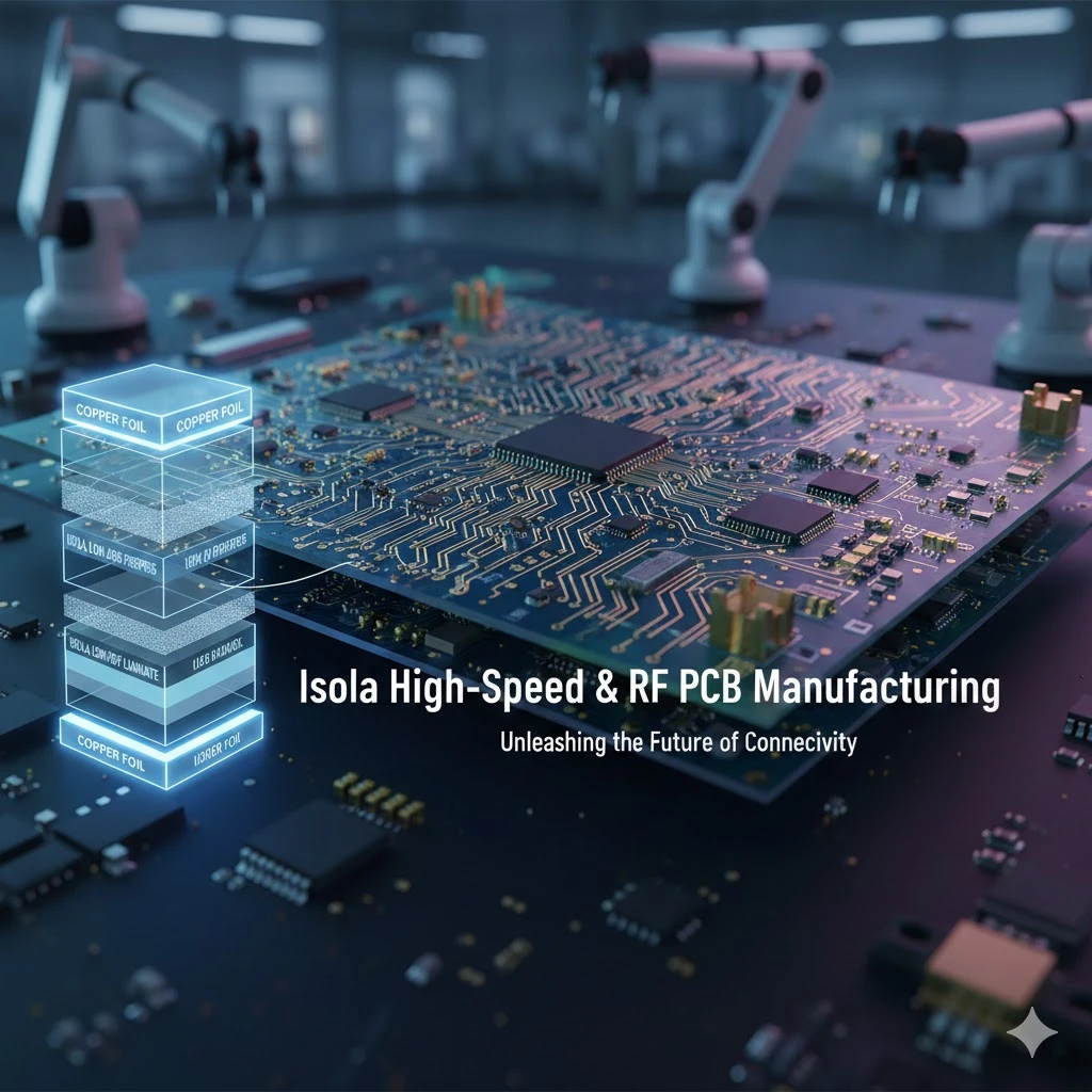
- Base Laminate (Dielectric): Specify low-loss materials such as Rogers RO4000 series (e.g., RO4350B, RO4003C) or Panasonic Megtron 6. Ensure the datasheet explicitly confirms the absence of ferromagnetic fillers sometimes used for flame retardancy.
- Dielectric Constant (Dk): Target a Dk between 3.0 and 3.7 (at 10 GHz) to minimize signal delay and crosstalk. Tolerance should be ±0.05.
- Dissipation Factor (Df): Ensure Df is < 0.005 to prevent signal attenuation and heat generation, which can be critical in the enclosed MRI bore environment.
- Surface Finish: Strictly specify Immersion Silver (ImAg) or Organic Solderability Preservative (OSP). Explicitly forbid ENIG (Electroless Nickel Immersion Gold) or ENEPIG, as the nickel layer is ferromagnetic.
- Copper Foil: Use Reverse Treated Foil (RTF) or Very Low Profile (VLP) copper to reduce conductor loss at high frequencies. Verify the copper purity is >99.9% to avoid ferrous impurities.
- Solder Mask: Use Low-Loss Solder Mask if possible. Standard green is acceptable, but ensure the pigment does not contain iron oxide. White or Black soldermasks often contain carbon or titanium dioxide, which are generally safe but should be verified for magnetic susceptibility.
- Via Plating: Specify "Non-magnetic Copper Plating" for via barrels. Ensure the plating bath chemistry is free of nickel additives often used for brightening.
- Impedance Control: Define single-ended impedance (usually 50Ω) and differential impedance (usually 100Ω or 90Ω) with a tolerance of ±5% rather than the standard ±10%.
- Layer Count & Stackup: For high-speed MRI coils, 4 to 8 layers are common. Use a symmetrical stackup to prevent warping, as MRI-compatible materials (like PTFE) can be mechanically softer than FR4.
- Thermal Reliability: Tg (Glass Transition Temperature) should be >170°C. MRI gradients generate significant heat; the material must not soften or outgas.
- Cleanliness: Specify ionic contamination levels < 0.75 µg/cm² NaCl equivalent. Residues can become conductive or reactive under high magnetic fields and RF excitation.
- Marking Ink: Ensure silkscreen ink is non-conductive and non-magnetic. Avoid metallic-based inks.
Manufacturing risks (root causes & prevention)
Defining specifications is only half the battle; understanding where the manufacturing process can silently introduce magnetic contamination is crucial for risk mitigation.
- Risk: Accidental Nickel Underplating
- Root Cause: The PCB fab house uses a shared plating line where nickel is standard for adhesion promotion (e.g., under Gold fingers).
- Detection: Use a handheld Gauss meter or strong rare-earth magnet on the bare board edges.
- Prevention: Explicitly state "NO NICKEL ALLOWED" in the fabrication notes and require a dedicated process route for your batch.
- Risk: Signal Integrity Loss due to Surface Finish
- Root Cause: Using HASL (Lead-Free) to avoid nickel results in uneven pads, causing impedance discontinuities for high-speed components.
- Detection: TDR (Time Domain Reflectometry) testing shows impedance mismatches at pad locations.
- Prevention: Mandate Immersion Silver, which is flat (planar) and non-magnetic, supporting high-speed signal integrity.
- Risk: Ferrous Contamination in Substrate
- Root Cause: Some "high-Tg" FR4 equivalents use fillers that have trace iron content for thermal stability.
- Detection: Susceptibility artifacts appear during the first MRI phantom test.
- Prevention: Use validated RF materials (Rogers/Isola) known for purity and request a Certificate of Conformance (CoC) for the specific laminate batch.
- Risk: Copper Roughness Attenuation
- Root Cause: Standard copper foil is roughened to adhere to the laminate, but this roughness increases skin effect losses at GHz frequencies.
- Detection: Insertion loss measurements (S21) are higher than simulated.
- Prevention: Specify VLP (Very Low Profile) or HVLP copper foil in the stackup.
- Risk: OSP Shelf Life Expiration
- Root Cause: OSP is organic and degrades/oxidizes rapidly if not stored in humidity-controlled environments.
- Detection: Poor wetting during reflow assembly; pads look discolored.
- Prevention: Enforce vacuum sealing with desiccant and humidity indicator cards; assemble within 6 months of fabrication.
- Risk: Silver Tarnish (Creep Corrosion)
- Root Cause: Immersion Silver reacts with sulfur in the air (or packaging materials) to form silver sulfide.
- Detection: Darkening or yellowing of pads.
- Prevention: Use sulfur-free paper for inter-leafing packaging and store in silver-safe bags.
- Risk: Thermal Expansion Mismatch (CTE)
- Root Cause: PTFE-based materials expand differently than copper vias (Z-axis expansion), leading to barrel cracks.
- Detection: Intermittent open circuits after thermal cycling.
- Prevention: Use hybrid stackups carefully or select "ceramic-filled" laminates that match copper's CTE closer than pure PTFE.
- Risk: Component Magnetism
- Root Cause: The PCB is perfect, but the assembly house uses standard capacitors with nickel barrier terminations.
- Detection: The assembled board is attracted to a magnet.
- Prevention: Specify "Non-Magnetic" passives (usually silver-palladium terminations) in the BOM and verify incoming components.
Validation & acceptance (tests and pass criteria)

To ensure the risks above have been managed, a rigorous validation plan must be executed before the boards are integrated into the MRI system.
- Magnetic Permeability Test:
- Objective: Confirm the bare PCB is non-magnetic.
- Method: Use a Severn Gauge or a high-sensitivity magnetometer (µ < 1.0001). Alternatively, a simple "hang test" with a strong neodymium magnet.
- Acceptance Criteria: Zero detectable attraction or deflection.
- Impedance Verification (TDR):
- Objective: Verify high-speed transmission lines meet design specs.
- Method: Time Domain Reflectometry on test coupons and actual traces.
- Acceptance Criteria: Measured impedance within ±5% of target (e.g., 50Ω ±2.5Ω).
- Insertion Loss Measurement:
- Objective: Confirm material loss tangent and copper roughness are within limits.
- Method: Vector Network Analyzer (VNA) sweep up to the operating frequency (e.g., 5 GHz).
- Acceptance Criteria: Loss (dB/inch) must not exceed the simulation budget by more than 10%.
- Solderability Test:
- Objective: Ensure the OSP or Silver finish is active and robust.
- Method: IPC-J-STD-003 wetting balance test.
- Acceptance Criteria: >95% coverage of the pad with fresh solder.
- Ionic Cleanliness Test:
- Objective: Prevent electrochemical migration in the humid MRI bore.
- Method: Rose Test or Ion Chromatography.
- Acceptance Criteria: < 0.75 µg NaCl eq./cm².
- Thermal Stress Test:
- Objective: Verify via reliability in Z-axis.
- Method: 6x solder float at 288°C (interconnect stress test).
- Acceptance Criteria: Change in resistance < 10%; no barrel cracks in microsection.
- Visual Inspection (High Magnification):
- Objective: Check for "Black Pad" (if using specialized finishes) or surface oxidation.
- Method: 100x optical microscopy.
- Acceptance Criteria: Uniform surface finish, no exposed copper, no tarnish.
- MRI Phantom Imaging (System Level):
- Objective: The ultimate functional test.
- Method: Place the PCB in the bore with a water phantom and run a standard sequence.
- Acceptance Criteria: Signal-to-Noise Ratio (SNR) degradation < 1%; no visible artifacts in the image.
Supplier qualification checklist (RFQ, audit, traceability)
When selecting a partner like APTPCB, use this checklist to ensure they have the specific capabilities for MRI-compatible manufacturing.
1. RFQ Inputs (What you must provide)
- Material Callout: Specific laminate (e.g., "Rogers RO4350B") or equivalent with "Non-Magnetic" explicitly stated.
- Surface Finish: "Immersion Silver" or "OSP" only. Note: "No Nickel".
- Impedance Table: Layer, trace width, spacing, and reference planes for all high-speed lines.
- Magnetic Constraint: A note on the fab drawing: "Class 3 Medical. Material and Plating must be Non-Magnetic. µr < 1.0001."
- Copper Profile: Request VLP or RTF copper if operating >1 GHz.
- Stackup Drawing: Detailed layer buildup including prepreg types.
- Drill Chart: Aspect ratios defined (keep < 10:1 for reliable plating without nickel).
- Solder Mask: "Low-loss" or standard, provided it is non-ferrous.
2. Capability Proof (What the supplier must show)
- Experience: Evidence of past medical/MRI PCB shipments.
- Plating Lines: Confirmation they have a dedicated Immersion Silver or OSP line (not shared with nickel processes that might cross-contaminate).
- Lamination: Ability to handle mixed-dielectric stackups (e.g., FR4 + PTFE) if a hybrid board is designed.
- Etching Precision: Capability for ±0.5 mil trace width tolerance for impedance control.
- Drilling: Mechanical and laser drilling capabilities for blind/buried vias in reinforced laminates.
- Handling: Procedures for handling silver-finished boards (gloves, sulfur-free paper).
3. Quality System & Traceability
- Certifications: ISO 13485 (Medical Devices) is highly preferred; ISO 9001 is mandatory.
- Material Traceability: Can they trace the laminate lot number to the specific PCB batch?
- CoC: Willingness to provide a Certificate of Conformance certifying "Non-Magnetic Construction".
- Inspection: Automated Optical Inspection (AOI) calibrated for silver/OSP reflectivity (which differs from HASL/ENIG).
- Impedance Reports: Sample TDR reports from previous high-speed runs.
- X-Ray: Availability of X-ray for layer registration verification.
4. Change Control & Delivery
- PCN Policy: Agreement to notify of any material or process change (e.g., changing solder mask brand) 6 months in advance.
- Packaging: Vacuum packing with desiccant and humidity indicators is mandatory.
- Shelf Life: Clear labeling of expiration date for OSP/Silver finishes.
- Scrap Policy: How do they handle boards that fail impedance tests? (They must be scrapped, not reworked).
- Logistics: Shock-proof packaging to prevent micro-fractures in brittle high-frequency laminates.
Decision guidance (trade-offs and decision rules)
Selecting the right combination of materials involves balancing signal performance, magnetic susceptibility, and cost.
- If you prioritize absolute signal integrity (>5 GHz): Choose Rogers RO4350B/RO4003C with Immersion Silver.
- Trade-off: Higher material cost and shorter shelf life for the finish compared to OSP.
- If you prioritize cost for lower-speed digital (<1 GHz): Choose High-Tg FR4 (Non-Magnetic Filler) with OSP.
- Trade-off: Higher dielectric loss (Df) than Rogers; OSP is harder to inspect visually than Silver.
- If you prioritize shelf life and assembly robustness: Choose Immersion Silver.
- Trade-off: Risk of tarnish if not stored correctly; slightly more expensive than OSP.
- If you prioritize thermal reliability (high power gradients): Choose Ceramic-filled PTFE laminates.
- Trade-off: Difficult to drill; requires experienced fabrication to prevent smear.
- If you need complex BGA mounting: Choose Immersion Silver.
- Trade-off: OSP can be uneven after multiple reflow cycles; Silver stays flatter.
- If you are considering ENIG for flatness: STOP.
- Rule: Never use ENIG for MRI bore applications. The nickel layer is magnetic. Use Silver instead.
FAQ (cost, lead time, Design for Manufacturability (DFM) files, testing)
Q: How much do high-speed MRI-compatible PCB materials increase the unit cost? A: Expect a 30% to 100% premium over standard FR4/ENIG boards.
- The base laminate (e.g., Rogers) is 3-5x the cost of FR4.
- Immersion Silver is generally comparable to ENIG but requires stricter handling.
- Testing (TDR, CoC) adds NRE (Non-Recurring Engineering) charges.
Q: What is the typical lead time for MRI-compatible PCB materials assembly? A: Standard lead time is 15–20 working days.
- Stock availability of specific Rogers/Megtron laminates can fluctuate; check stock before ordering.
- Quick-turn (5-7 days) is possible if materials are in stock at the fab.
Q: What DFM files are required for high-speed MRI-compatible PCB materials? A: Beyond standard Gerbers, you must provide:
- IPC-356 Netlist (for electrical test verification).
- Stackup diagram with target impedance values.
- Readme file explicitly stating "NON-MAGNETIC REQUIREMENTS".
Q: Can I use standard FR4 if I only need MRI compatibility but not high speed? A: Yes, but you must still control the surface finish.
- Standard FR4 is usually non-magnetic (verify fillers).
- You must still specify OSP or Immersion Silver to avoid Nickel plating.
Q: How do you test for magnetic compliance during production? A: We use a "Go/No-Go" magnet test on the production line.
- High-sensitivity Gauss meters are used for QA sampling.
- Visual inspection ensures no nickel-based components or plating anomalies.
Q: What are the acceptance criteria for high-speed MRI-compatible PCB materials testing? A: The board must pass three gates:
- Magnetic: Zero attraction to a calibrated magnet.
- Electrical: Impedance within ±5% or ±10% as specified.
- Visual: No tarnish on Silver/OSP pads.
Q: Why is Immersion Silver preferred over Immersion Tin for MRI? A: Silver has higher conductivity and better planarity.
- Tin can form "whiskers" over time, risking shorts.
- Silver is better suited for high-frequency skin-effect conduction.
Q: Do I need special solder paste for MRI-compatible PCB materials assembly? A: The paste itself is usually standard SAC305 (Lead-Free).
- However, ensure the flux residues are non-corrosive (No-Clean is preferred).
- Verify that the component terminations (caps/resistors) are non-magnetic (Silver/Palladium), not the paste itself.
Related pages & tools
- Medical PCB Manufacturing: Explore our specific capabilities for medical devices, including ISO 13485 compliance and traceability.
- High-Speed PCB Design: Deep dive into impedance control, signal integrity, and material selection for gigabit transmission.
- Rogers PCB Materials: Detailed specs on Rogers laminates, the industry standard for low-loss, high-frequency applications.
- PCB Surface Finishes: Compare Immersion Silver, OSP, and other finishes to understand their impact on shelf life and assembly.
- DFM Guidelines: Download our design rules to ensure your MRI-compatible board is manufacturable at scale.
Request a quote (Design for Manufacturability (DFM) review + pricing)
Ready to validate your design? Send us your data for a comprehensive DFM review that checks for both signal integrity and magnetic compliance risks.
What to include in your quote request:
- Gerber Files (RS-274X)
- Fabrication Drawing (with "Non-Magnetic" and "No Nickel" notes clearly visible)
- Stackup & Impedance Requirements
- Bill of Materials (BOM) if assembly is required (highlighting non-magnetic passives)
- Estimated Annual Volume
Click here to Request a Quote & DFM Review – Our engineering team will review your stackup for high-speed performance and MRI safety within 24 hours.
Conclusion (next steps)
Successfully deploying high-speed MRI-compatible PCB materials requires a disciplined approach that merges RF engineering with strict material science controls. It is not enough to simply select a low-loss laminate; you must rigorously exclude nickel from the plating process, validate the non-magnetic properties of every layer, and ensure the surface finish supports the signal speeds you require. By following the specifications, risk mitigation strategies, and supplier checklists outlined in this playbook, you can confidently move from prototype to production, ensuring your medical device delivers clear images and reliable data every time.