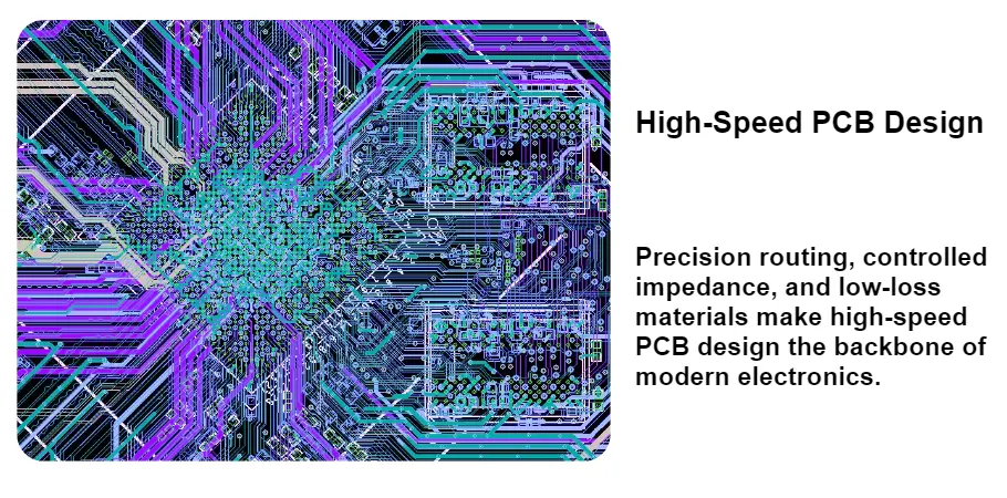
If you’re searching for high-speed PCB design, you’re likely trying to solve one of these problems: DDR timing instability, a PCIe/SerDes eye that won’t open, unexpected EMI failures, or boards that pass basic testing but fail under real load. High-speed success is rarely a single “routing trick.” It comes from a complete set of decisions that stay consistent from stack-up definition to final verification.
At APTPCB, we help teams turn high-speed designs into manufacturable, testable hardware by aligning stack-up, impedance targets, materials, and fabrication control. If you need a production capability reference, see high-speed PCB.
Menu Navigation
To make this guide easy to use, here is a structured directory that follows the real workflow engineers apply in high-speed PCB design:
- 1) When a PCB Becomes High-Speed
- 2) Stack-Up and Impedance Control
- 3) Routing Rules for DDR and SerDes
- 4) 10 Layout Tips You Can Use Today
- 5) Power Integrity and EMI Control
- 6) Simulation and Manufacturing Validation
1. When a PCB Becomes High-Speed
A board becomes “high-speed” when edge rate (rise/fall time) is fast enough that traces behave like transmission lines. Even if the clock frequency looks moderate, fast edges make impedance discontinuities and return-path breaks visible in the waveform.
What typically fails first in high-speed PCB design
- Reflections and ringing: Caused by impedance mismatch at vias, pads, connectors, neck-downs, and layer transitions.
- Crosstalk: Field coupling between adjacent traces injects noise into victim nets, shrinking the eye and increasing jitter.
- Broken return paths: Routing across plane splits or moving between layers without a controlled reference transition forces return current detours, raising loop inductance and EMI.
- Skew and timing margin loss: Unequal propagation delay and asymmetric discontinuities break DDR setup/hold and multi-lane alignment.
- PI-driven SI issues: PDN noise shifts thresholds and references, turning a “good route” into a failing system.
Design takeaway: high-speed PCB design is system engineering—SI, PI, and EMI are linked by geometry and return currents.
2. Stack-Up and Impedance Control
In high-speed PCB design, stack-up is the foundation. It determines whether controlled impedance is achievable and whether return paths are stable. Routing rules cannot “fix” a stack-up that lacks continuous reference planes or forces excessive layer transitions.
For complex platforms, lock the structure early using a defined PCB stack-up.
Stack-up rules that create stable high-speed behavior
- Tight coupling to a reference plane: Place high-speed signal layers adjacent to a continuous ground plane to minimize loop inductance and confine fields.
- Prefer stripline for critical links: Internal stripline offers better shielding and reduces radiation compared to external microstrip.
- Avoid plane splits under high-speed nets: A split breaks the return path and turns the trace into an antenna loop.
- Pair power and ground planes when possible: Plane pairing increases distributed capacitance and reduces PDN impedance at high frequency.
- Minimize layer changes on the fastest nets: Each layer transition is a discontinuity plus a return-path event.
Controlled impedance that stays consistent in production
Controlled impedance is about continuity, not a single “50Ω/100Ω number.” To keep impedance consistent along the whole channel:
- Keep trace width/spacing stable wherever possible
- Avoid abrupt neck-downs unless required for pad escape
- Control solder mask effects on microstrip (it changes effective dielectric)
- Define impedance coupons and tolerance, then verify using TDR
For higher layer counts used in compute, communications, and industrial platforms, many designs use multilayer PCB structures to balance planes, routing density, and manufacturability.
3. Routing Rules for DDR and SerDes
Most practical high-speed PCB design questions are about routing. The goal is straightforward:
Protect the return path, preserve impedance, and control coupling. Length matching matters—but only within the interface budget and topology requirements.
Differential pairs (PCIe, USB, Ethernet, SerDes)
- Maintain constant spacing to keep differential impedance stable.
- Route pairs symmetrically (same number of vias, same layer changes, same structures).
- Avoid obstacles between the pair (vias, copper voids, stitching that breaks symmetry).
- Keep pair geometry consistent through breakout and connector regions.
- Length tune only as needed; excessive meanders increase loss and coupling risk.
DDR routing (data/strobe/clock/address)
- Follow required topology first (fly-by and termination strategy drive the layout).
- Match within functional groups: DQ↔DQS, CK relationships, and addr/cmd budgets.
- Control stubs and branching; avoid “antenna-like” extensions on critical nets.
- Keep reference planes continuous under the bus.
- Isolate and protect clocks from aggressors.
Crosstalk control that works in dense layouts
- Avoid long parallel runs; if unavoidable, break coupling length with layer changes or spacing.
- Route adjacent layers orthogonally where practical.
- Prefer stripline for the most sensitive links when spacing is constrained.
- Keep aggressors away from clocks, resets, and high-impedance nodes.
If your product includes RF blocks alongside high-speed digital, consider dedicated RF structures such as high-frequency PCB for the RF region while keeping the digital stack optimized for DDR/SerDes.
4. 10 Layout Tips You Can Use Today
Sometimes you don’t need a new theory—you need a quick review checklist before tapeout. The following “quick wins” are production-friendly layout habits that reduce the most common SI/PI/EMI failure modes in high-speed PCB design.
High-speed PCB design checklist
- Route high-speed signals over a continuous ground plane to stabilize impedance and return paths.
- Avoid clustering too many vias in one area (via farms can choke planes and concentrate current density).
- Avoid sharp 90° corners; use 45° angles or smooth arcs to reduce discontinuities and manufacturing risk.
- Increase spacing between adjacent high-speed traces to reduce coupling; if a bottleneck is unavoidable, expand spacing immediately after it.
- Avoid long stubs/branches; use cleaner topologies to prevent reflections and antenna-like behavior.
- Route differential pairs with constant spacing and symmetry, and don’t place obstacles between the pair.
- Keep via transitions symmetric in differential links (same number of vias, same structures) and minimize via count overall.
- Do not route high-speed signals across split planes; if reference changes are required, provide an intentional return-current path.
- Separate analog and digital grounds intentionally for mixed-signal designs, connecting them in a controlled way at a defined point.
- Match trace geometry thoughtfully at component interfaces to reduce impedance “steps” at pads and transitions.
Use this list as a fast design review step, then verify the highest-risk nets with simulation and measurement.
5. Power Integrity and Electromagnetic Interference (EMI) Control
High-speed PCB design fails when power and reference planes move. A stable waveform depends on a stable reference, and that depends on a low-impedance PDN and controlled return current behavior.
PDN goals for real high-speed performance
- Low impedance across frequency: avoid impedance peaks that align with switching harmonics.
- Low inductance at the load: placement and via strategy matter more than adding “more capacitors.”
- Small loop areas: minimize switching loop size to reduce noise and EMI.
Decoupling strategy (practical, not theoretical)
- Place high-frequency decaps close to power pins with short connections to planes.
- Use tight via pairs (power/ground) to reduce mounting inductance.
- Combine bulk + mid + high-frequency capacitors intentionally.
- Avoid isolating decaps behind long traces or narrow neck-downs.
EMI control through return-path discipline
- Keep high-speed routing over continuous reference planes.
- Avoid crossing plane splits and voids.
- Plan layer transitions so return currents have a nearby path (stitching strategy near transitions when needed).
- Reduce common-mode conversion by keeping differential structures symmetric.
For dense, performance-driven builds where process control is crucial (tight impedance, advanced vias, strict registration), early alignment with advanced PCB manufacturing practices reduces scaling risk.
6. Simulation and Manufacturing Validation
High-speed PCB design should be predictive: simulate early, then validate what you actually built. The goal is to avoid “trial-and-error hardware” by catching risk before fabrication—and then confirming compliance after manufacturing.
What to check before you release the design
- Stack-up feasibility: can you hit impedance targets with realistic trace geometry?
- Link sensitivity: which discontinuities dominate (vias, connectors, packages, pad transitions)?
- Crosstalk hotspots: dense escape, long parallel routes, tuning meanders.
- PDN risk: decoupling effectiveness and impedance trends.
- Return-path continuity: identify every reference change and confirm the return path is controlled.
What to validate after fabrication
- Controlled impedance measurement using test coupons (TDR targets and tolerances).
- Stack-up build confirmation (dielectric thickness, copper weight, registration).
- Repeatability controls before volume production (process alignment across lots).
For consistency from prototype to volume, align your release package with the PCB fabrication process so manufacturing parameters match the assumptions used in your SI/PI planning.
Conclusion
A production-ready high-speed PCB design follows a clear workflow: define stack-up first, control impedance and return paths, route DDR/SerDes with symmetry and coupling control, design the PDN to keep reference planes stable, and validate both in simulation and in manufacturing.
If you need support building high-speed boards that can scale reliably from prototype to production, APTPCB provides controlled impedance fabrication and verification through high-speed PCB.