- Treat Gerber review as a quote-readiness check, not as a public PCB price calculator.
- Fabrication data can reveal board structure, drill and routing complexity, and where the package still needs engineering notes before RFQ.
- A stable quote still depends on inputs that Gerbers do not carry by themselves: BOM scope, stack-up intent, finish duty, build stage, and validation context.
Quick Answer You can estimate how much review a PCB package is likely to need from Gerber data, but you cannot settle the full commercial answer from Gerbers alone. A fabrication package can reveal board outline, layer and drill complexity, dense routing regions, and visible process-sensitive features. It cannot by itself define component sourcing, released stack-up intent, finish purpose, whether the build is still a prototype or already production-intent, or what validation and test expectations belong with the RFQ.
Table of Contents
- What should be reviewed first?
- What can Gerber review tell you before RFQ?
- What can Gerber review not answer alone?
- Which review triggers are visible in fabrication data?
- What is a safe workflow before RFQ?
- Where do prototype, BOM, and quote pages fit?
- What should be included with the package?
- Next steps
- FAQ
What should be reviewed first?
Before asking what a board should cost, settle four boundaries:
- Is the request bare-board only, or will assembly and BOM scope affect the answer?
- Is the build still a validation prototype, a production-intent prototype, or a controlled RFQ release package?
- Are the Gerbers being used to understand fabrication complexity, or are they being treated as a substitute for the rest of the release package?
- Is schedule urgency part of the request, or is the real question simply whether the package is quote-ready?
Those boundaries matter because many cost discussions go off track when Gerber review, build purpose, and schedule posture are blended into one vague question.
| Review boundary | What it answers | What it does not prove |
|---|---|---|
| Fabrication data | What the board geometry, copper artwork, and drill structure appear to require | Final pricing by itself |
| Build purpose | Whether the next build is mainly for validation or for a more controlled release step | That the package is already ready for a stable quote |
| Schedule posture | Whether the request may need accelerated handling after review | That every board is suitable for the same schedule category |
| Package completeness | Whether the Gerbers are supported by the notes needed for RFQ | That no engineering clarification will be needed |
What can Gerber review tell you before RFQ?
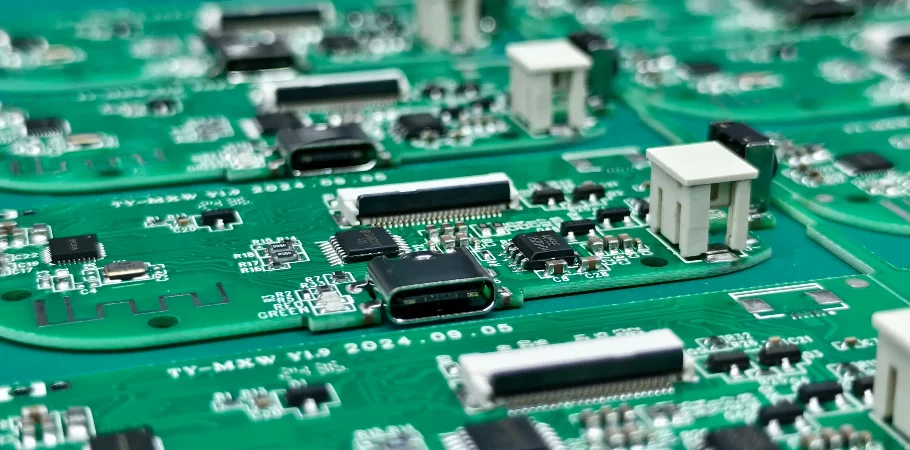
Gerber review is valuable because it exposes the physical shape of the design package early.
Before RFQ, a reviewer can usually confirm or flag:
- board outline, dimensions, cutouts, and edge features
- visible layer set and copper distribution
- dense breakout or routing zones that may need closer review
- drill count, mixed hole styles, slots, and obvious via-family complexity
- whether the package appears complete enough for engineering intake
- whether the artwork suggests a baseline multilayer route or a more specialized process discussion
What can Gerber review not answer alone?
The main gaps are not technical mistakes in the Gerbers. They are missing inputs that belong outside the Gerber set.
| Missing input | Why it must stay separate | What Gerber data cannot settle |
|---|---|---|
| BOM and sourcing posture | Assembly cost and release risk depend on exact parts, alternates, and supply ownership | Whether the assembly scope is stable |
| Stack-up intent | Material family, impedance planning, thickness direction, and layer roles belong in released notes | The approved electrical and material build |
| Finish duty | Contact wear, solderability, flatness, or special pad use can change finish selection | Which finish should be assumed |
| Build stage | A validation prototype and a production-intent package may carry different commercial assumptions | Why the build exists and how controlled it already is |
| Validation context | Coupons, inspection, programming, or test expectations may affect the package review | What evidence the build is expected to produce |
One of the most common quoting disasters starts when a buyer or engineer drags only the bare-board Gerber set into an automatic quote tool and accepts the result as if it were real commercial truth. The algorithm sees a multilayer outline, visible routing density, and ordinary drill artwork, then returns an attractive standard multilayer number such as $500. The trap is that Gerber alone does not reliably define drill pairs or special copper weight. The failure appears only after order release, when CAM opens the fabrication drawing or the IPC-D-356 netlist and discovers the hidden structure: this is not a standard multilayer board at all, but a Hidden HDI trap with Blind/Buried Vias and 2 oz internal copper. The real manufacturing cost is closer to $3000. What follows is not a small correction. It is a re-quote, a Budget blowout, and often a schedule collapse while special materials or lamination capacity are rechecked. The commercial damage is as real as the engineering miss. The customer loses weeks, the budget owner loses credibility, and the supplier relationship starts with a preventable trust failure. This is why Gerber-only pricing is a gamble. Without stackup definition, fabrication notes, and process intent, the quote is not firm. It is bait for later correction.
Which review triggers are visible in fabrication data?
The practical way to discuss how to estimate pcb cost from gerber is to focus on review triggers rather than on a pretend calculator.
| Fabrication-data trigger | Why it usually prompts deeper review | What should be added before RFQ |
|---|---|---|
| Dense breakout or tightly packed routing regions | Fine-feature areas may move the package into closer fabrication and assembly review | Stack-up notes and any assembly-sensitive context |
| Multiple drill families, slots, or unusual hole structures | Mixed drilling and hole treatment often need clearer process notes | Fabrication drawing notes and released drill intent |
| Via-in-pad, blind-via, or buried-via cues | The artwork may imply special structures that need explicit confirmation | Via treatment notes and controlled stack-up definition |
| Contact fingers or exposed wear surfaces | Finish cannot safely be guessed from geometry alone | Finish requirement and where it applies |
| Embedded array or panel assumptions | Quote scope can change if the release package is really a single board versus an array-managed build | Panel ownership or array instruction |
| Incomplete outline or inconsistent file set | Missing release detail creates quote churn before manufacturing review can stabilize | One controlled revision package |
The real failure chain is usually package ambiguity, not a hidden calculator formula: Gerbers show a real board, but stackup, finish, BOM, or build-stage ownership remains implicit -> the reviewer makes or delays assumptions during intake -> engineering query loops or re-quotes appear after the RFQ has already started -> schedule slips while the release package is rebuilt.
What is a safe workflow before RFQ?
Use Gerber review as an intake check, then add the missing commercial and engineering context around it.
1. Check the fabrication package itself
Confirm that the Gerbers, drill data, outline, and revision references describe one real board state.
2. Mark the review triggers that the artwork exposes
If the files show dense routing, special vias, unusual holes, contact areas, or array assumptions, treat those as prompts for supporting notes, not as pricing answers.
3. Add the non-Gerber inputs explicitly
Release the stack-up intent, finish requirement, BOM boundary, build-stage note, and any validation context that affects the build.
4. Separate build purpose from schedule posture
Prototype describes why the build exists. It is about validation, iteration, or production-intent learning. Quick-turn describes schedule urgency after review. It is not the same thing, and Gerber upload alone does not settle either decision.
5. Move to RFQ only after one package describes one intent
The stronger package is not the one with the biggest file set. It is the one where fabrication data, notes, and release context all point to the same build.
Where do prototype, BOM, and quote pages fit?
Use the related pages according to the gap that is still open:
- PCB Prototype when the main question is build purpose: validation prototype, production-intent prototype, or NPI-oriented handoff.
- Components & BOM when the Gerbers are readable but the commercial answer is still unstable because the BOM, alternates, or sourcing boundary are not controlled.
What should be included with the package?
If you want Gerber review to become a cleaner RFQ handoff, send:
- Gerber files, NC drill files, and revision-controlled fabrication references
- stack-up intent when layer roles, thickness direction, material choice, or impedance matter
- finish requirements, especially if contact zones or assembly-sensitive pad conditions are involved
- BOM and sourcing posture if assembly is included or expected to affect the quote
- a clear build-stage note such as validation prototype, production-intent prototype, or released RFQ package
- validation or inspection context if the build is expected to support specific review or test evidence
- any separate schedule request stated as schedule posture, not blended into the build-purpose label
Next steps with APTPCB
If you are trying to budget a complex multilayer board, an HDI design, or a high-frequency stackup and you are already tired of auto-quoters producing suspiciously low numbers that later turn into bait-and-switch pricing, stop asking Gerber-only tools to make a promise they cannot keep. The real quoting question is whether the hidden cost drivers have been exposed before procurement and schedule commitments are made.
Send the full RFQ package, including Gerber, ODB++, fabrication drawing, BOM, and any special process requirements, to sales@aptpcb.com or through the quote page.
APTPCB's NPI quoting engineers will return a firm, risk-assessed quote within 24 hours. We will identify hidden cost drivers, verify the real manufacturing burden of Blind/Buried Vias and lamination structure, and give you a quote that can survive budget review instead of collapsing into a late re-price after the CAM team opens the real package.
FAQ
Can I get an exact PCB price from Gerber files alone?
No. Gerbers can reveal fabrication complexity and quote-review triggers, but they do not define the full commercial answer by themselves.
Do Gerber files tell me whether the board is prototype or production?
No. Gerbers describe the board data. Prototype, production-intent, and release posture are decisions about build purpose and control level around that data.
Is prototype the same thing as quick-turn?
No. Prototype is a build-purpose label. Quick-turn is a schedule posture after review. A board can be a prototype without automatically belonging in the same schedule category as a simpler approved build.
When does the BOM page matter more than more Gerber review?
When the fabrication package already looks readable, but the commercial answer still depends on exact MPNs, approved alternates, sourcing ownership, or package consistency for assembly.
What is the safest handoff after a Gerber self-check?
Send one controlled package that combines the fabrication data with stack-up, finish, BOM, build-stage, and validation notes, then use the quote page once those inputs are aligned.
Public references
IPC-2581 Consortium, "What is IPC-2581?" Supports the digital-package framing used when a Gerber-only handoff is insufficient for a stable RFQ.
APTPCB PCB Prototype page Supports the build-stage boundary used to separate validation prototype, production-intent prototype, and RFQ release posture.
APTPCB Components and BOM page Supports the sourcing-boundary discussion used when Gerbers alone cannot stabilize the commercial answer.
APTPCB DFM Guidelines Supports the pre-RFQ package review posture used when the file set still needs engineering clarification.
Author and review information
- Author: APTPCB quoting, release-package, and DFM content team
- Technical review: RFQ-intake, fabrication-review, and document-control engineering team
- Last updated: 2026-05-15