Interpreting a Time Domain Reflectometry (TDR) report is the final verification step between a fabricated Printed Circuit Board (PCB) and a functional high-speed system. For technical buyers and quality engineers, this report serves as the certificate of compliance, confirming that the physical stackup and etching processes met the strict signal integrity requirements defined in the design phase.
Highlights
- What to specify upfront (data, stackup, materials, testing).
- Key risks and early detection signals.
- Validation plan and pass/fail criteria.
- Supplier qualification checklist and RFQ inputs.
Key Takeaways
- What to specify upfront (data, stackup, materials, testing).
- Key risks and early detection signals.
- Validation plan and pass/fail criteria.
- Supplier qualification checklist and RFQ inputs.
- Standard Tolerance: Most standard rigid PCBs target $\pm$10% impedance tolerance; tighter control (Class 3 or high-speed) often demands $...
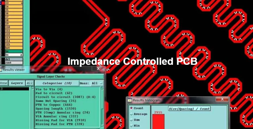
- The Coupon Concept: TDR testing is destructive to the test pads; therefore, manufacturers test a "coupon" (a replica circuit on the panel...
- The "Launch" Artifact: The first 200–500 picoseconds (ps) of the graph represent the probe connecting to the coupon and should be ignored...
Highlights
- Standard Tolerance: Most standard rigid PCBs target $\pm$10% impedance tolerance; tighter control (Class 3 or high-speed) often demands $\pm$5%.
- The Coupon Concept: TDR testing is destructive to the test pads; therefore, manufacturers test a "coupon" (a replica circuit on the panel border) rather than the live board.
- The "Launch" Artifact: The first 200–500 picoseconds (ps) of the graph represent the probe connecting to the coupon and should be ignored when reading the impedance value.
- Measurement Zone: The valid measurement window is the flat "plateau" in the middle of the graph, typically representing 3 to 6 inches of trace length.
- Environmental Factors: Temperature and humidity can shift impedance values by 1–2 Ohms; ensure testing occurs in a controlled environment.
- Correlation: A passing coupon guarantees the process was correct, but design errors (e.g., missing reference planes on the actual board) can still cause system failure.
- Validation Tip: Always verify that the trace width on the physical coupon matches the cross-section report to ensure the TDR data is authentic.
Contents
- Scope, Decision Context, and Success Criteria
- Specifications to Define Upfront (Before You Commit)
- Key Risks (Root Causes, Early Detection, Prevention)
- Validation & Acceptance (Tests and Pass Criteria)
- Supplier Qualification Checklist (RFQ, Audit, Traceability)
- How to Choose (Trade-Offs and Decision Rules)
- FAQ (Cost, Lead Time, DFM Files, Materials, Testing)
- Glossary (Key Terms)
Scope, Decision Context, and Success Criteria
When sourcing an impedance controlled PCB, the TDR report is not just a formality; it is the primary data point proving the board will function at frequency. This playbook covers the interpretation of these reports for rigid, flex, and rigid-flex circuits.
Success Criteria
To consider a TDR validation successful, the following metrics must be met:
- Impedance Compliance: All tested lines fall within the specified tolerance (e.g., 50 $\Omega$ $\pm$5 $\Omega$).
- Waveform Stability: The TDR trace shows a stable impedance plateau without significant inductive spikes or capacitive dips exceeding 2–3 $\Omega$ within the test region.
- Process Capability: For volume production, the Cpk (Process Capability Index) for impedance should be $\ge$ 1.33, indicating statistically stable manufacturing.
Boundary Cases
- Short Traces: Traces shorter than 1.5 inches are difficult to measure accurately with standard TDR probes due to the "launch" reflection masking the reading.
- High-Loss Materials: On standard FR4, long traces may show an upward slope in impedance due to DC resistance and dielectric loss; this requires a specific "slope correction" or interpretation method.
Specifications to Define Upfront (Before You Commit)
A readable TDR report starts with a clear fabrication drawing. If the requirements are ambiguous, the manufacturer may use a "best effort" approach that passes their internal checks but fails your system requirements.
Critical Fabrication Notes
Include these specific requirements in your RFQ and Fab Drawing:
- Impedance Models: Clearly list every controlled line (e.g., "Layer 1, 50 Ohm SE, 5 mil width").
- Test Frequency/Rise Time: Specify the rise time for the TDR pulse. Standard is often 200ps or 500ps. For high-speed applications (25Gbps+), request a faster rise time (e.g., 35ps).
- Coupon Design: Mandate that coupons must be designed per IPC-2221 guidelines and must remain attached to the panel until final inspection.
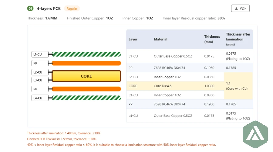
- Dielectric Materials: Specify the exact material family (e.g., Isola PCB or Rogers) to fix the Dielectric Constant (Dk).
- Reference Planes: Explicitly state which layers are ground references. Ambiguity here is the #1 cause of stackup errors.
Key Parameters Table
| Parameter | Standard Spec | High-Performance Spec | Why it Matters |
|---|---|---|---|
| Impedance Tolerance | $\pm$10% | $\pm$5% | Determines signal reflection margin. |
| Trace Width Tolerance | $\pm$20% | $\pm$10% or $\pm$0.5 mil | Etching variations directly alter impedance. |
| Dielectric Height | $\pm$10% | $\pm$5% | Distance to ground plane is the strongest impedance driver. |
| Copper Thickness | IPC Class 2 | IPC Class 3 | Plating thickness affects signal propagation speed. |
| Test Coupon | Vendor Standard | IPC-2221 Type Z | Ensures the test vehicle matches the PCB geometry. |
| TDR Rise Time | < 200 ps | < 50 ps | Faster rise time reveals smaller discontinuities. |
| Dk Tolerance | $\pm$5% | $\pm$2% | Material consistency ensures batch-to-batch repeatability. |
| Moisture Content | < 0.2% | < 0.1% | Water absorption lowers impedance (water Dk $\approx$ 80). |
Key Risks (Root Causes, Early Detection, Prevention)
Understanding how to read impedance coupon TDR report data requires recognizing what failure looks like. Most failures stem from physical manufacturing deviations.
1. Over-Etching (High Impedance)
- Root Cause: The chemical etchant removed too much copper, making the trace narrower than designed. A 0.5 mil reduction in width can raise impedance by 2–4 Ohms.
- Early Detection: The TDR graph shows a flat line, but it is consistently above the target value (e.g., hovering at 58 $\Omega$ for a 50 $\Omega$ target).
- Prevention: Implement strict PCB fabrication process controls and use "etch compensation" on the artwork (swelling traces by 0.5–1.0 mil).
2. Prepreg Thickness Variation (Low Impedance)
- Root Cause: During lamination, resin flows out more than expected, reducing the distance between the trace and the reference plane.
- Early Detection: The TDR graph is stable but consistently below the target.
- Prevention: Use "low-flow" prepregs or verify the PCB stack-up press cycle parameters.
3. Impedance Discontinuities (the "Dip")
- Root Cause: Localized capacitance increases, often caused by a via stub, a component pad, or a change in reference plane (e.g., crossing a split plane).
- Early Detection: A sharp downward spike in the TDR waveform.
- Prevention: Ensure continuous return paths in the design. For the manufacturer, ensure plating is uniform.
4. Fiber Weave Effect
- Root Cause: In loose weave glass (like 106 or 1080 style), a trace may run on top of a glass bundle (high Dk) and then over a resin gap (low Dk).
- Early Detection: The TDR line looks "wavy" or periodic rather than flat.
- Prevention: Use spread glass FR4 or zigzag routing for critical high-speed lines.
5. Coupon-to-Board Mismatch
- Root Cause: The coupon design does not match the actual board geometry (e.g., different ground pour clearance).
- Early Detection: The coupon passes, but the actual board fails functional testing.
- Prevention: Perform a "microsection" analysis on the actual PCB to verify it matches the coupon geometry.
6. Moisture Absorption
- Root Cause: The PCB absorbed moisture from the air before testing.
- Early Detection: Impedance reads generally lower than expected across all layers.
- Prevention: Bake boards before testing and store in vacuum-sealed bags.
7. Probe Contact Issues
- Root Cause: Dirty probes or poor contact pressure on the test pad.
- Early Detection: The "launch" section of the graph is noisy or shows a massive inductive spike (>10 $\Omega$).
- Prevention: Clean probes regularly and use automated TDR machines (e.g., Polar Atlas).
8. Lamination Voids
- Root Cause: Air trapped between layers changes the effective Dk (Air Dk = 1.0).
- Early Detection: Unpredictable, sharp spikes in impedance; often accompanied by delamination.
- Prevention: Optimize vacuum lamination pressure and dwell time.
Validation & Acceptance (Tests and Pass Criteria)
When you receive the TDR report, do not just look for the "PASS" stamp. Analyze the waveform data.
The Anatomy of a TDR Waveform
- Region 1: The Launch (0 – 0.5 ns): This is the cable and probe connecting to the coupon. You will see a disturbance. Ignore this.
- Region 2: The Test Trace (0.5 ns – End): This is the "Device Under Test" (DUT). This line should be flat.
- Region 3: The Open (End): The line shoots up to infinity (open circuit) at the end of the coupon trace.
Acceptance Criteria Checklist
| Test Item | Acceptance Criteria | Sampling Plan |
|---|---|---|
| Mean Impedance | Must be within tolerance (e.g., 50 $\Omega$ $\pm$10%). | 100% of coupons (usually 2 per panel). |
| Impedance Variation | The line should not ripple more than $\pm$2 $\Omega$ within the test region. | All tested lines. |
| Trace Width Verification | Physical width must match the design $\pm$20% (or specified tolerance). | 1 microsection per lot. |
| Layer Alignment | Layer-to-layer registration < 5 mil deviation. | 1 microsection per lot. |
| Dk Verification | Calculated Dk from TDR must match material spec $\pm$5%. | Periodic audit. |
| Test Length | Valid data window must cover at least 60% of the coupon length. | Visual check of graph. |
How to Validate the Report Data
- Check the Scale: Manufacturers sometimes change the Y-axis scale to make a wavy line look flat. Ensure the scale is typically 2–5 Ohms per division, not 20.
- Check the Date/Time: Ensure the report was generated after the final plating process.
- Verify the Stackup: Compare the stackup used in the report (dielectric heights) against your design. If they adjusted the dielectric thickness by more than 10% to hit impedance, it might violate your mechanical constraints.
Supplier Qualification Checklist (RFQ, Audit, Traceability)
Before awarding a contract for impedance controlled PCB production, verify the supplier's capabilities.
- Equipment: Does the vendor use industry-standard TDR equipment (e.g., Polar CITS880s, Tektronix DSA8300, or Agilent)?
- Software: Do they use a field solver (e.g., Polar SI8000 or SI9000) for stackup calculation, or simple approximation formulas?
- Coupon Generation: Is the coupon generation automated based on the CAM data, or manually drawn (high risk of error)?
- Traceability: Can they link a specific TDR graph to a specific manufacturing panel and date code?
- Data Retention: Do they archive TDR data for at least 2 years?
- Material Stock: Do they stock the specific high-speed materials (e.g., Megtron or Rogers) required, or will they substitute?
- Etch Compensation: Do they have a documented procedure for calculating etch factors based on copper weight?
- Environment: Is the testing lab temperature and humidity controlled?
- Calibration: Is the TDR equipment calibrated annually with traceable standards?
- DFM Support: Do they offer a DFM review to suggest stackup adjustments before fabrication?
- Class 3 Capability: Can they demonstrate capability for IPC Class 3 impedance tolerance ($\pm$5%)?
- Probe Maintenance: Is there a log for probe tip replacement? (Worn probes give noisy data).
How to Choose (Trade-Offs and Decision Rules)
Deciding on the strictness of impedance control involves balancing cost against signal integrity risk.
- If the interface is standard USB 2.0 or slow GPIO (< 100 MHz), choose standard PCB fabrication without specific TDR reporting (design for 50 $\Omega$, but don't pay for testing).
- If the interface is DDR3/DDR4, PCIe Gen 3, or Ethernet (1Gbps+), choose $\pm$10% tolerance with 100% TDR testing.
- If the interface is PCIe Gen 5, 56G PAM4, or high-frequency RF (> 5GHz), choose $\pm$5% tolerance and specify low-roughness copper.
- If budget is a primary constraint, choose to test only the most critical single-ended and differential lines, rather than every controlled line on the board.
- If the board is a Rigid-Flex PCB, choose a vendor with specific experience in hatched-ground impedance control, as solid planes are rare in flex regions.
- If you are using HDI PCB technology (microvias), choose a vendor who can place coupons that include microvia structures to test the actual signal path.
- If the trace width is < 4 mil, choose a supplier with Laser Direct Imaging (LDI) capability to ensure etch accuracy.
- If the stackup is asymmetrical, choose to relax the bow/twist tolerance, as impedance control requires strict dielectric thicknesses that may cause warping.
- If you need Quick Turn PCB service, choose standard materials (FR4) over exotic RF materials to avoid lead time delays, provided the loss budget allows it.
- If the TDR report shows a failure, choose to review the cross-section. If the geometry is correct but impedance is wrong, the material Dk may be the culprit.
FAQ (Cost, Lead Time, DFM Files, Materials, Testing)
Q: How much does impedance testing add to the PCB cost? A: Typically, impedance control and TDR reporting add 5% to 15% to the board cost. This covers the extra CAM engineering time, the coupon space on the panel, and the labor for testing.
Q: Can a failed impedance board be reworked? A: No. Once the traces are etched and layers laminated, the geometry is fixed. If the impedance is out of spec, the boards must be scrapped and re-manufactured with adjusted etch compensation or dielectric thickness.
Q: Why does the TDR line go up at the end of the trace? A: An "open" circuit (the end of the trace) has infinite impedance. The TDR graph will shoot vertically upward at the point where the trace ends. This confirms the signal traveled the full length of the coupon.
Q: What is the difference between Single-Ended and Differential TDR? A: Single-ended measures one line relative to ground (typically 50 $\Omega$). Differential measures the interaction between two coupled lines (typically 90 $\Omega$ or 100 $\Omega$). Differential testing requires a TDR with two synchronized pulses.
Q: Why do my short traces fail TDR? A: Traces shorter than 1.5 to 2 inches are often buried in the "launch" reflection of the probe. It is physically difficult to get a clean reading. For these, rely on the manufacturer's process control on longer traces on the same layer.
Q: Does solder mask affect impedance? A: Yes. Solder mask reduces impedance by 2–3 Ohms because it has a higher dielectric constant (Dk $\approx$ 3.5) than air (Dk = 1.0). The manufacturer's calculation must account for whether the trace is coated or exposed.
Q: What is "impedance tolerance: what pcb fabs can realistically hold"? A: Standard fabs hold $\pm$10%. Advanced fabs with LDI and automated lamination can hold $\pm$5%. Anything tighter (e.g., $\pm$2%) is generally considered experimental or requires extremely expensive selection processes.
Q: Can I use a standard multimeter to measure impedance? A: No. A multimeter measures DC resistance (Ohms). Impedance is AC resistance at a specific frequency. You must use a TDR or Vector Network Analyzer (VNA).
Request a Quote / DFM Review for How to Read Impedance Coupon TDR Report (What to Send)
Glossary (Key Terms)
| Term | Definition |
|---|---|
| TDR (Time Domain Reflectometry) | A measurement technique that sends a fast pulse down a line and measures reflections to calculate impedance. |
| Coupon | A test circuit located on the manufacturing panel rail, designed to represent the actual PCB traces. |
| Characteristic Impedance ($Z_0$) | The ratio of voltage to current for a wave propagating along a transmission line. |
| Differential Pair | Two complementary signals used to transmit data, offering high noise immunity. |
| Dielectric Constant (Dk / $\epsilon_r$) | A measure of a material's ability to store electrical energy; affects signal speed and impedance. |
| Loss Tangent (Df) | A measure of signal power lost as heat within the dielectric material. |
| Rise Time | The time it takes for a signal to go from 10% to 90% of its final value; faster rise times require better impedance control. |
| Microstrip | A trace on an outer layer, separated from a single reference plane by dielectric. |
| Stripline | A trace on an inner layer, sandwiched between two reference planes. |
| Etch Factor | The ratio of etch depth to lateral etch (undercut); critical for calculating final trace width. |
| Launch | The interface between the TDR probe and the test coupon; creates a noise artifact at the start of the graph. |
| DUT (Device Under Test) | The specific component or trace being measured. |
Conclusion (Next Steps)
Mastering how to read impedance coupon TDR report data transforms you from a passive buyer into an active quality partner. By defining clear specs upfront—specifically the test rise time, coupon design, and tolerance class—you prevent costly signal integrity failures. Remember, the TDR graph is the heartbeat of your high-speed PCB; a flat, stable line within the $\pm$10% (or $\pm$5%) window is the ultimate sign of a healthy manufacturing process. For your next high-speed project, ensure your PCB manufacturing partner has the equipment and transparency to provide this level of validation.