Contents
- Highlights
- How to Reduce PCB Cost without Sacrificing Yield: Definition and Scope
- How to Reduce PCB Cost without Sacrificing Yield Rules and Specifications
- How to Reduce PCB Cost without Sacrificing Yield Implementation Steps
- How to Reduce PCB Cost without Sacrificing Yield Troubleshooting
- 6 Essential Rules for How to Reduce PCB Cost without Sacrificing Yield (Cheat Sheet)
- FAQ
- Request a Quote / DFM Review for How to Reduce PCB Cost without Sacrificing Yield
- Conclusion
As a Senior CAM Engineer at APTPCB, I review hundreds of Gerber files every week. The most common conversation I have with designers isn't about whether a board can be built, but whether it should be built that way given the budget constraints. Learning how to reduce pcb cost without sacrificing yield is the holy grail of electronics manufacturing. It requires a strategic balance between Design for Manufacturing (DFM) principles, material selection, and understanding the physical limitations of the fabrication process. It is not about cutting corners; it is about removing "invisible costs"—specifications that drive up price without adding performance or reliability.
Quick Answer
To effectively master how to reduce pcb cost without sacrificing yield, you must focus on standardizing your design to fit within "standard capability" rather than "advanced capability" wherever possible. This minimizes the need for specialized equipment, reduces scrap rates, and accelerates throughput.
- Standardize Materials: Stick to standard TG150-170 FR4 unless high-speed/RF requirements strictly dictate otherwise.
- Optimize Panelization: Aim for >80% material utilization. Waste laminate is paid for by you, even if it ends up in the bin.
- Minimize Drill Counts: Reduce the number of different drill sizes. Each tool change adds machine time.
- Relax Tolerances: If a mechanical hole doesn't need +/- 0.05mm, allow +/- 0.10mm. Tighter tolerances increase inspection time and fallout.
- Avoid HDI if Possible: Blind and buried vias require sequential lamination cycles, which can double or triple the cost compared to through-hole designs.
- Verification: Always run a DFM check to identify "cost drivers" like annular rings below 4mil or trace/space below 4mil before quoting.
Highlights
- Material Utilization: The single biggest hidden cost is poor panel efficiency; optimizing board size to fit standard production panels (e.g., 18"x24") can save 20-30%.
- Layer Count Logic: Reducing layer count saves money, but not if it forces you into expensive HDI technology to route the signals.
- Surface Finish Strategy: ENIG is reliable but expensive; OSP or HASL are cost-effective alternatives for boards without fine-pitch BGAs.
- Via Management: Minimizing the aspect ratio (board thickness vs. drill diameter) prevents expensive plating issues and reliability failures.
How to Reduce PCB Cost without Sacrificing Yield: Definition and Scope
When we discuss how to reduce pcb cost without sacrificing yield, we are essentially talking about risk management and resource allocation. The price of a Printed Circuit Board (PCB) is derived from three main factors: Material Costs (the laminate and copper), Process Costs (machine time, plating baths, lamination cycles), and Yield Loss (the percentage of boards that fail quality control).
Many designers focus solely on the material, thinking that making the board smaller always makes it cheaper. However, if shrinking the board forces you to use 3mil/3mil trace/space width or laser micro-vias, the Process Cost and Yield Loss will skyrocket, negating any material savings.
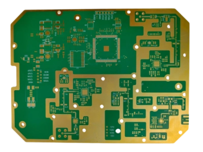
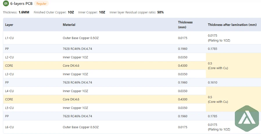
True cost reduction comes from keeping your design within the "sweet spot" of manufacturing capabilities. For example, a standard FR4 PCB with 5mil lines and spaces is significantly cheaper to produce than one with 3mil lines, simply because the etching yield is near 100% for the former and lower for the latter. Similarly, understanding the impact of your stackup is crucial. A 4-layer board is standard, but an odd-layer count (e.g., 5 layers) can cause warping issues that ruin yield, effectively increasing the price per usable board.
Below is a decision matrix that helps visualize how specific technical levers impact the practical cost and yield of your project.
Tech / Decision Lever → Practical Impact
| Decision Lever / Spec | Practical Impact (Yield/Cost/Reliability) |
|---|---|
| Panel Utilization | High Impact. Poor utilization (<70%) means you pay for waste. Adjusting board dimensions by millimeters can often fit more units per panel. |
| Via Technology | Critical Cost Driver. Through-holes are standard. Blind/Buried vias require extra lamination cycles (+40-60% cost). |
| Trace / Space Width | Yield Driver. Standard ≥5mil is safe. <3.5mil requires specialized etching and inspection, increasing scrap risk and cost. |
| Surface Finish | Cost vs. Assembly. HASL is cheapest but not flat. ENIG is flat but pricey. OSP is cheap and flat but has short shelf life. |
| Drill Count & Size | Machine Time. >1000 holes or <0.2mm mechanical drills increase CNC time and drill bit breakage risk. |
How to Reduce PCB Cost without Sacrificing Yield Rules and Specifications
To systematically apply cost reduction, you need to adhere to specific design rules. These rules keep your board in the "standard" processing category at APTPCB, avoiding the surcharges associated with "advanced" or "complex" manufacturing.
The following table outlines the recommended specifications for a cost-optimized design.
| Rule | Recommended Value | Why it matters | How to verify |
|---|---|---|---|
| Min Trace / Space | ≥ 5mil / 5mil (0.127mm) | Going below 4mil reduces etching yield and requires finer dry film, increasing cost. | Run DRC (Design Rule Check) in your CAD tool. |
| Min Mechanical Drill | ≥ 0.25mm (10mil) | Drills smaller than 0.2mm break easily, slowing down the CNC process and increasing tool costs. | Check the drill table in your CAM software. |
| Annular Ring | ≥ 5mil (pad vs hole) | Ensures the drill hits the pad even with slight misalignment. Prevents "breakout" which scraps the board. | Verify pad diameter is at least 10mil larger than hole size. |
| Layer Count | Even Numbers (2, 4, 6...) | Odd layer counts (e.g., 3, 5) cause warping during lamination due to asymmetrical copper balance. | Review your PCB Stackup configuration. |
| Board Thickness | 1.6mm (Standard) | Non-standard thicknesses (e.g., 2.0mm, 0.8mm) may require special laminate ordering or handling. | Check board properties. |
| Copper Weight | 1oz (35µm) | Heavy copper (>2oz) requires more etching time and wider spacing, increasing complexity. | Specify 1oz unless current handling requires more. |
Adhering to these rules ensures that your board flows through the factory without stopping for special engineering queries (EQ) or requiring specialized machine setups.
How to Reduce PCB Cost without Sacrificing Yield Implementation Steps
Implementing these strategies requires a structured approach during the design phase. It is much harder to reduce cost after the design is locked. Follow this process to ensure how to reduce pcb cost without sacrificing yield is baked into your workflow.
Implementation Process
Step-by-step execution guide
Start by defining the simplest stackup that meets your signal integrity needs. Use standard FR4 (TG150) materials. Avoid defining specific brands (e.g., "Isola 370HR") unless necessary; allow the fab to use "IPC-4101 equivalent" to leverage their stock inventory.
Place components to minimize trace lengths and crossing. This reduces the need for extra layers and vias. Prioritize routing on outer layers to reduce the need for expensive blind/buried vias. Keep traces ≥5mil where density allows.
Consult with your manufacturer about their standard working panel sizes (e.g., 18x24 inches). Adjust your PCB dimensions or array layout to maximize the number of boards per panel. A 5mm reduction might allow an extra row of boards.
Before finalizing, run a comprehensive DFM check. Look for "cost adders" like peelable mask, carbon ink, or hard gold if they aren't strictly needed. Consolidate drill sizes to reduce tool changes.
How to Reduce PCB Cost without Sacrificing Yield Troubleshooting
Even with the best intentions, issues can arise. Here are common problems that occur when trying to cut costs aggressively, and how to fix them without blowing the budget.
1. Warpage and Bowing
The Issue: To save money, a designer might remove copper pours from signal layers or use an asymmetrical stackup (e.g., different prepreg thicknesses on top vs. bottom). This causes the board to warp during reflow soldering. The Fix: Always maintain a symmetrical stackup relative to the center of the board. Use copper flooding (thieving) on empty areas of signal layers to balance the copper density. This adds virtually no cost but significantly improves yield and flatness.
2. Solder Mask Misalignment
The Issue: Specifying very thin solder mask dams (e.g., <3mil) between pads to support fine-pitch components on a standard-cost board. The Fix: If you cannot afford the high-precision alignment required for 3mil dams, use "gang relief" (grouping mask openings) for fine-pitch headers, or increase the spacing between pads if possible. This prevents solder bridging without paying for premium alignment capabilities.
3. Poor Plating in Vias
The Issue: Using small vias (0.2mm) on a thick board (2.0mm or more). This creates a high aspect ratio (>10:1), making it difficult for the plating solution to coat the inside of the hole reliably. The Fix: Keep the aspect ratio below 8:1 for standard cost. If you need a thick board, use larger vias (0.3mm+). If you need small vias, reduce the board thickness. This ensures reliable connectivity without requiring specialized plating cycles.
For more detailed guidelines on avoiding these pitfalls, refer to our DFM Guidelines.
6 Essential Rules for How to Reduce PCB Cost without Sacrificing Yield (Cheat Sheet)
| Rule / Guideline | Why It Matters (Physics/Cost) | Target Value / Action |
|---|---|---|
| Standardize Laminate | Exotic materials have long lead times and high MOQs. Standard FR4 is stocked in bulk. | FR4 TG150 (IPC-4101) |
| Maximize Panel Usage | You pay for the whole panel. Low utilization = paying for scrap. | >80% Utilization |
| Consolidate Drills | Every tool change takes time. CNC machine time is a major cost factor. | <10 Unique Sizes |
| Avoid Blind/Buried Vias | Requires sequential lamination (multiple press cycles), drastically increasing cost. | Through-Hole Only |
| Relax Tolerances | Tight tolerances (e.g., +/- 2mil routing) require slower machining and higher scrap. | +/- 0.10mm (Routing) |
| Surface Finish Choice | Gold is expensive. If flat pads aren't needed, use cheaper options. | HASL or OSP (if viable) |
FAQ
Q: Does reducing the number of layers always reduce the cost?
A: Generally, yes. A 4-layer board is cheaper than a 6-layer board. However, if reducing layers forces you to use HDI technology (micro-vias) or extremely fine traces (3mil) to route the connections, the cost will actually increase. It is often cheaper to add two layers than to use HDI.
Q: Is OSP cheaper than ENIG?
A: Yes, OSP (Organic Solderability Preservative) is significantly cheaper than ENIG (Electroless Nickel Immersion Gold). However, OSP has a shorter shelf life and is more sensitive to handling. For simple boards or high-volume consumer electronics, OSP is a great way to learn how to reduce pcb cost without sacrificing yield.
Q: How does the quantity ordered affect the unit price?
A: PCB manufacturing has high setup costs (tooling, film generation, machine setup). In Mass Production, these setup costs are amortized over thousands of units, dropping the unit price drastically. For prototypes, you are paying mostly for setup.
Q: Can I use a non-rectangular shape to save money?
A: Usually, no. While you can design any shape, rectangular boards panelize the most efficiently. Odd shapes often leave unusable gaps on the production panel, increasing material waste.
Request a Quote / DFM Review for How to Reduce PCB Cost without Sacrificing Yield
Ready to optimize your next project? At APTPCB, we specialize in helping customers balance performance with budget. Send us your data for a free DFM and cost-reduction analysis.
What to send for an accurate quote:
- Gerber Files: RS-274X format preferred.
- Drill File: Excellon format with a tool list.
- Stackup Diagram: Specify layer order and copper weight.
- Fabrication Drawing: Include notes on color, finish, and tolerances.
- Quantities: Prototype (e.g., 5-10) vs. Production (e.g., 1000+).
Conclusion
Mastering how to reduce pcb cost without sacrificing yield is not about choosing the cheapest materials or the lowest-quality fab house. It is about smart engineering—optimizing your design to fit standard manufacturing processes, maximizing material utilization, and avoiding unnecessary complexity. By following the rules of thumb regarding trace width, drill sizes, and stackups, you can achieve a high-yield, reliable product at a competitive price point.
Signed, The Engineering Team at APTPCB