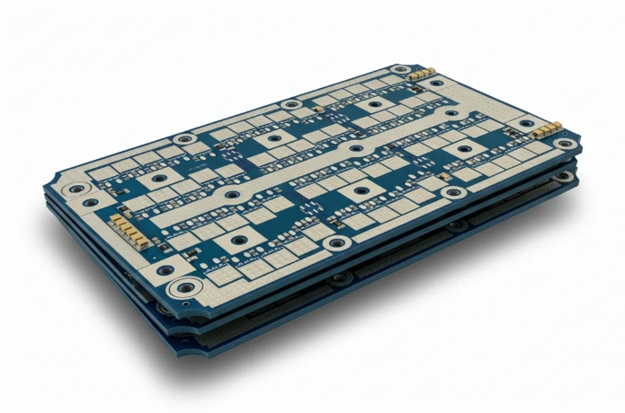
High Power Amplifier (HPA) circuits represent one of the most challenging intersections in electronics manufacturing: the convergence of high-frequency signal integrity and extreme thermal management. Unlike standard logic boards, an HPA PCB must transmit delicate RF signals while simultaneously dissipating the intense heat generated by power transistors. For engineers and procurement teams, success lies in balancing dielectric properties with mechanical robustness.
At APTPCB (APTPCB PCB Factory), we see firsthand how slight deviations in material selection or copper plating can lead to catastrophic amplifier failure. This guide serves as a central hub for understanding the lifecycle of these critical boards, from initial design parameters to final quality validation.
Key Takeaways
Before diving into the technical nuances of amplifier board fabrication, here are the critical points that define successful production.
- Definition: HPA PCBs are specialized circuit boards designed to support High Power Amplifiers, requiring both low-loss RF performance and high thermal conductivity.
- Thermal Metric: The most critical non-electrical metric is Thermal Conductivity (W/mK); standard FR4 is often insufficient for the active device areas.
- Signal Metric: Dielectric Constant (Dk) stability over temperature is vital to prevent phase shifts during high-power operation.
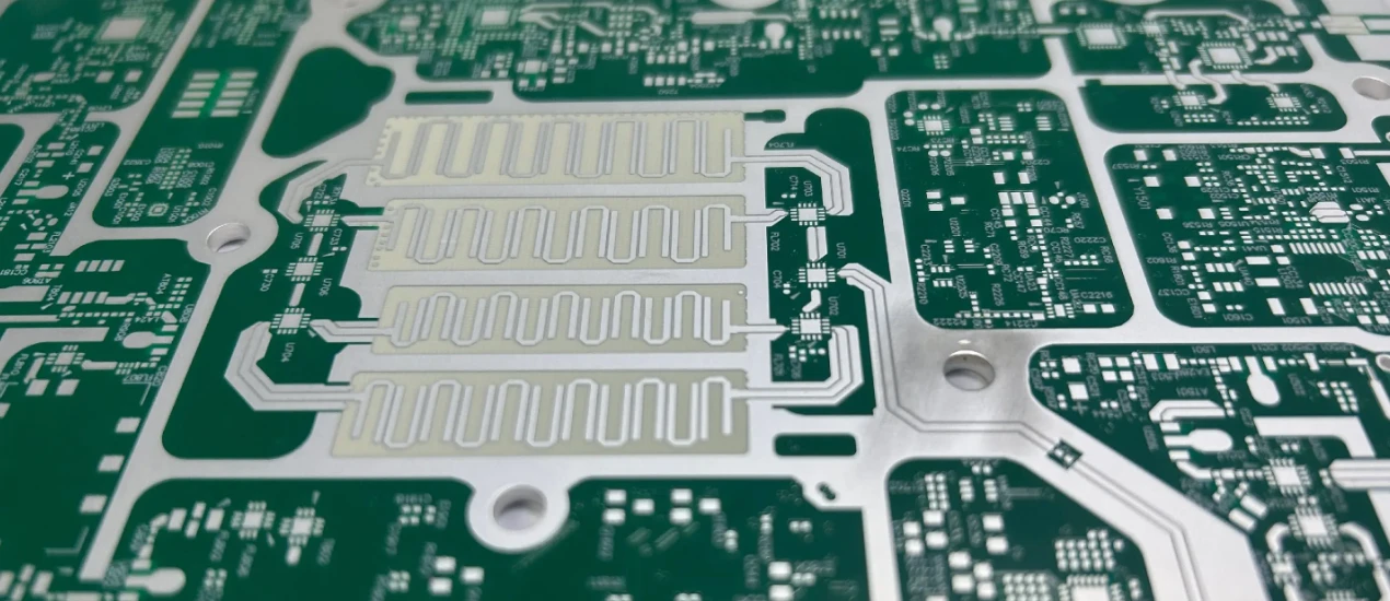
- Copper Weight: Heavy copper (2oz+) is common for power rails, but surface roughness must be controlled to minimize skin effect losses on signal lines.
- Misconception: "High Tg" does not automatically mean "High Thermal Conductivity." They measure different properties (mechanical stability vs. heat transfer).
- Tip: Use embedded copper coins or heavy via farms directly under GaN or GaAs transistors to shunt heat away immediately.
- Validation: X-ray inspection is mandatory for checking void percentages under QFN or localized heat sinks, as voids block heat transfer.
What High Power Amplifier (HPA) PCB really means (scope & boundaries)
Building on the core takeaways, it is essential to define exactly what falls under the category of an HPA PCB to avoid manufacturing mismatches.
An HPA PCB is not simply a power supply board, nor is it a standard RF board; it is a hybrid that manages the stress of both. These boards are the backbone of systems like Block Converter PCB assemblies, satellite uplinks, and radar transmitters. The "High Power" in this context refers to RF power (watts to kilowatts of RF energy), not just DC voltage.
The scope of HPA PCB manufacturing includes:
- Thermal Management: The board must act as a heat exchanger. The active devices (often Gallium Nitride or Gallium Arsenide) generate rapid heat spikes that must move through the Z-axis of the board to a chassis or heatsink.
- Frequency Range: These boards often operate from the L-band up to the Ka-band. This requires materials that do not absorb signal energy as heat.
- Mechanical Stability: High power creates thermal cycles. The board materials must expand and contract at rates (CTE) compatible with the soldered components to prevent solder joint cracking.
Common applications include BUC PCB (Block Upconverter) units used in VSAT terminals and solid-state power amplifiers (SSPA) for defense and telecommunications. If a board only handles high DC current but low-speed signals, it is a Power PCB. If it handles high frequency but low power (milliwatts), it is a standard RF PCB. The HPA PCB must handle both.
High Power Amplifier (HPA) PCB metrics that matter (how to evaluate quality)
Once the scope is defined, engineers must quantify performance using specific metrics that predict how the board will behave under load.
The following table outlines the physical and electrical properties that dictate the reliability of an HPA PCB. At APTPCB, we recommend specifying these values clearly in your fabrication notes rather than just listing a brand name, as this allows for flexible yet compliant manufacturing.
| Metric | Why it matters for HPA | Typical Range / Factor | How to Measure |
|---|---|---|---|
| Thermal Conductivity (Tc) | Determines how fast heat moves away from the amplifier chip. Low Tc leads to overheating and gain drift. | 0.3 W/mK (FR4) to 380 W/mK (Copper Coin). High-performance laminates: 1.0–3.0 W/mK. | ASTM D5470 or Laser Flash method. |
| Dielectric Constant (Dk) | Affects impedance and signal velocity. In HPAs, Dk must remain stable as the board heats up. | 2.2 to 10.2 (depending on design size). Tolerance ±0.05 is standard. | IPC-TM-650 2.5.5.5 (Clamped Stripline). |
| Dissipation Factor (Df) | Measures how much signal is lost as heat within the substrate. High power + High Df = Burnt board. | < 0.0025 (Low Loss) to < 0.0009 (Ultra Low Loss). | IPC-TM-650 2.5.5.5. |
| Tg (Glass Transition Temp) | The temperature where the board turns soft. HPA boards run hot, so high Tg prevents mechanical failure. | > 170°C (High Tg) to > 280°C (Polyimide/PTFE). | DSC (Differential Scanning Calorimetry). |
| Td (Decomposition Temp) | The temperature where the material physically degrades/loses weight. Critical for assembly reliability. | > 340°C is recommended for lead-free assembly. | TGA (Thermogravimetric Analysis). |
| CTE-Z (Expansion) | How much the board expands in thickness. High expansion breaks plated through-holes (PTH). | < 50 ppm/°C (ideal). PTFE can be higher, requiring care. | TMA (Thermomechanical Analysis). |
| Peel Strength | Bond strength between copper and dielectric. High heat can weaken this bond, causing delamination. | > 0.8 N/mm (Standard). > 1.0 N/mm preferred for high thermal stress. | IPC-TM-650 2.4.8. |
How to choose High Power Amplifier (HPA) PCB: selection guidance by scenario (trade-offs)
Understanding the metrics is the first step; applying them to specific real-world scenarios requires balancing performance against cost and manufacturability.
Different HPA applications prioritize different metrics. A BUC PCB for a satellite dish has different needs than a radar module. Below are six common scenarios and the recommended approach for each.
1. Satellite Uplink (Ku/Ka-Band BUC)
- Scenario: Continuous wave (CW) transmission, outdoor environment, high frequency (12–30 GHz).
- Priority: Low loss (Df) and environmental stability.
- Recommendation: Use PTFE-based laminates (like Rogers RT/duroid or Taconic TLY) reinforced with woven glass.
- Trade-off: PTFE is soft and difficult to process (drilling smear). It requires specialized plasma etching.
- APTPCB Insight: For cost savings, use a hybrid stackup: PTFE on the top layer for RF, and FR4 for the bottom control layers.
2. 5G Base Station Power Amplifier
- Scenario: High volume, moderate power, cost-sensitive.
- Priority: Thermal conductivity and price.
- Recommendation: Hydrocarbon ceramic laminates (like Rogers RO4350B or Isola I-Tera). These process like FR4 but offer better RF performance.
- Trade-off: Not as low-loss as pure PTFE, but significantly cheaper to assemble.
3. Military Radar (Pulse Power)
- Scenario: Extremely high peak power, pulsed operation, harsh vibration.
- Priority: Thermal capacity and mechanical bond strength.
- Recommendation: Metal Core PCB (MCPCB) or boards with embedded copper coins. The metal base acts as an infinite heatsink.
- Trade-off: Heavy weight and limited multilayer capabilities compared to standard laminates.
4. Industrial Heating / RF Energy
- Scenario: Lower frequency (ISM bands like 915 MHz or 2.4 GHz), very high raw power.
- Priority: Copper weight and current carrying capacity.
- Recommendation: Thick copper (3oz or 4oz) on high-Tg FR4 or mid-range RF material.
- Trade-off: Fine line etching is impossible with thick copper. Design must accommodate wider spacing.
5. Avionics Communication
- Scenario: Space-constrained, weight-sensitive, moderate power.
- Priority: Size reduction and reliability.
- Recommendation: HDI PCB techniques using laser microvias to route signals in tight spaces, combined with high-performance thin dielectrics.
- Trade-off: Higher fabrication cost due to sequential lamination cycles.
6. Lab Test Equipment (SSPA)
- Scenario: Controlled environment, ultra-wideband performance.
- Priority: Flat frequency response over a wide band.
- Recommendation: Liquid Crystal Polymer (LCP) or ultra-low profile copper foil materials.
- Trade-off: Material availability can be scarce; lead times are often longer.
High Power Amplifier (HPA) PCB implementation checkpoints (design to manufacturing)
After selecting the right approach for your scenario, the focus shifts to the tactical execution of the design through the manufacturing line.
To ensure the final HPA PCB performs as simulated, specific checkpoints must be verified during the PCB fabrication process.
1. Material Stock Verification
Risk: High-performance laminates (Rogers, Arlon, Taconic) often have long lead times or specific thickness availability. Action: Confirm stock with the manufacturer before freezing the stackup. Do not assume standard FR4 thicknesses (e.g., 1.6mm) apply to RF materials.
2. Hybrid Stackup Design
Risk: Mixing materials (e.g., PTFE and FR4) causes warping due to different CTE values. Action: Ensure the stackup is symmetrical. Use "no-flow" prepreg for bonding to prevent resin from flowing onto RF pads during lamination.
3. Copper Roughness Selection
Risk: At high frequencies, current travels on the surface (skin effect). Rough copper acts like a resistor, increasing heat and loss. Action: Specify "VLP" (Very Low Profile) or "HVLP" (Hyper Very Low Profile) copper foil for the RF layers.
4. Thermal Via Management
Risk: Standard vias are insufficient for HPA heat loads. Action: Implement dense via farms under components. Request via plugging with conductive epoxy (VIPPO) or cap plating to provide a flat soldering surface for the power transistor.
5. Embedded Coin Integration
Risk: If the copper coin is not bonded correctly, air gaps will insulate the heat source. Action: Define the tolerance for the coin protrusion/recession (typically +/- 25um). The coin must be flush with the surface for good thermal contact.
6. Etching Compensation
Risk: High power lines are often wide, while RF lines are precise. Action: The CAM engineer must apply different etching compensation factors for thick copper layers to maintain impedance control.
7. Surface Finish Selection
Risk: HASL (solder) has poor planarity and high RF loss. ENIG (Gold) can be brittle (black pad) or lossy due to nickel. Action: Use Immersion Silver (best for RF, but tarnishes) or ENEPIG (universal, but expensive). For pure HPA, Immersion Silver is often preferred for its conductivity.
8. Solder Mask Application
Risk: Solder mask adds dielectric loss and can affect impedance. Action: Remove solder mask from high-frequency traces (solder mask opening). If protection is needed, use a specific low-loss solder mask ink.
9. Profiling and Routing
Risk: Mechanical stress can crack ceramic-filled laminates. Action: Use specialized router bits and optimized feed speeds. Ensure edges are free of burrs which can cause arcing in high-voltage HPA applications.
High Power Amplifier (HPA) PCB common mistakes (and the correct approach)
Even with a solid plan, specific pitfalls frequently trip up engineering teams when moving from prototype to production.
Avoiding these common errors can save weeks of debugging and thousands of dollars in scrap.
Ignoring CTE Mismatch:
- Mistake: Bonding a ceramic-filled PTFE layer to a standard FR4 layer without considering that they expand at different rates during reflow.
- Result: Delamination or bowed boards that cannot be assembled.
- Correction: Use high-Tg FR4 that is matched as closely as possible to the RF material, or use a balanced construction.
Over-Specifying Tolerances:
- Mistake: Requesting +/- 5% impedance tolerance on a standard power trace where +/- 10% is sufficient.
- Result: Unnecessary cost increases and lower yield.
- Correction: Only apply strict tolerances to the RF signal path.
Neglecting Plating Thickness in Thermal Calculations:
- Mistake: Calculating thermal resistance based on the barrel of the via but ignoring the plating thickness.
- Result: The vias act as a bottleneck for heat.
- Correction: Specify a minimum wall thickness (e.g., 25um or 1 mil) for thermal vias, or request filled vias.
Using Standard FR4 for >2GHz High Power:
- Mistake: Assuming FR4 works because the frequency is "only" 2.4GHz.
- Result: The resin heats up due to dielectric loss, darkening the board and shifting the impedance, eventually causing failure.
- Correction: Use Rogers PCB materials or similar low-loss options for the active layers.
Poor Grounding Strategies:
- Mistake: Insufficient stitching vias around the HPA circuit.
- Result: Parasitic inductance and radiation, leading to self-oscillation of the amplifier.
- Correction: Place grounding vias as close as possible (lambda/20 spacing) to shield the RF path.
Late DFM Engagement:
- Mistake: Designing a complex coin-embedded board and sending it for quote without prior consultation.
- Result: The design is unmanufacturable or requires expensive re-tooling.
- Correction: Send a preliminary stackup to APTPCB early in the design phase.
High Power Amplifier (HPA) PCB FAQ (cost, lead time, materials, testing, acceptance criteria)
Addressing the most frequent questions regarding the logistics and technical validation of HPA boards.
Q: What is the primary cost driver for HPA PCBs? A: The laminate material is the biggest factor. PTFE and ceramic-filled materials can cost 5x to 10x more than FR4. The second driver is complexity, such as embedded copper coins or sequential lamination for blind/buried vias.
Q: How does lead time compare between standard PCBs and HPA PCBs? A: Standard PCBs take days; HPA PCBs often take 2–4 weeks. This is primarily due to material procurement (if not in stock) and the slower, more careful processing required for soft RF materials.
Q: Can I use a "Hybrid Stackup" to save money? A: Yes. A hybrid stackup uses expensive RF material only for the top signal layer and cheaper FR4 for the remaining layers (power, ground, control). This is the standard approach for cost-effective Block Converter PCB designs.
Q: What testing is required for HPA PCBs? A: Beyond standard E-test (Open/Short), HPA boards often require Hi-Pot testing (for high voltage breakdown), Impedance TDR testing, and sometimes PIM (Passive Intermodulation) testing if specified.
Q: What are the acceptance criteria for thermal vias? A: For IPC Class 2, some voiding in the via fill is acceptable. However, for HPA applications, we recommend IPC Class 3 requirements for plated through-holes to ensure maximum thermal transfer reliability.
Q: How do I specify a copper coin in my Gerber files? A: Create a separate mechanical layer outlining the coin profile. Clearly indicate in the fabrication drawing whether the coin is "embedded" (inside the board), "press-fit," or "bonded."
Q: Why is Immersion Silver preferred over ENIG for HPA? A: Nickel (in ENIG) is ferromagnetic and has higher resistance, which can cause signal loss and heating at high frequencies. Silver is highly conductive and non-magnetic, making it ideal for RF signals.
Q: What is the maximum power an HPA PCB can handle? A: There is no single limit; it depends on the cooling design. A properly designed board with a copper coin and liquid cooling can handle kilowatts. A standard PCB without cooling may fail at 50 Watts.
Resources for High Power Amplifier (HPA) PCB (related pages and tools)
To further assist in your design and procurement process, we have curated a list of related capabilities and tools available at APTPCB.
- Material Data: Deep dive into High Frequency PCB materials to compare Rogers, Taconic, and Isola options.
- Thermal Solutions: Learn more about Metal Core PCB technology for heat dissipation.
- Design Tools: Use our Impedance Calculator to estimate trace widths for your specific dielectric material.
- General Capability: Review our full PCB Capabilities to understand minimum trace widths and drill sizes.
High Power Amplifier (HPA) PCB glossary (key terms)
A quick reference guide to the technical terminology used in High Power Amplifier PCB manufacturing.
| Term | Definition |
|---|---|
| BUC (Block Upconverter) | A device used in satellite transmission that converts a band of frequencies from a lower frequency to a higher frequency. |
| Copper Coin | A solid piece of copper embedded into the PCB to provide a direct thermal path from a component to the heatsink. |
| CTE (Coefficient of Thermal Expansion) | The rate at which a material expands when heated. Mismatches cause reliability issues. |
| Dk (Dielectric Constant) | The ratio of the permittivity of a substance to the permittivity of free space. Affects signal speed. |
| Df (Dissipation Factor) | A measure of loss-rate of energy of a mode of oscillation in a dissipative system. Lower is better for HPA. |
| Hybrid Stackup | A PCB construction that combines different materials (e.g., FR4 and PTFE) to balance cost and performance. |
| PIM (Passive Intermodulation) | Signal distortion that occurs when two or more signals mix in a non-linear device (or poor PCB junction). |
| Skin Effect | The tendency of high-frequency alternating current to distribute itself within the conductor so that the current density is largest near the surface. |
| Thermal Via | A via used specifically to transfer heat from one layer to another, often filled with conductive material. |
| TDR (Time Domain Reflectometry) | A measurement technique used to determine the characteristic impedance of a trace. |
| VLP Copper | Very Low Profile copper foil with low surface roughness, used to minimize signal loss at high frequencies. |
| Weave Effect | Signal variation caused by the periodic structure of the glass weave in the laminate. |
Conclusion (next steps)
Successfully manufacturing an HPA PCB requires a shift in mindset from "connectivity" to "performance stability." Whether you are building a Block Converter PCB for satellite comms or a radar module, the interaction between heat, frequency, and material science cannot be ignored.
To move forward with your project, ensure your data package is complete. When submitting a design for DFM review or quotation to APTPCB, please include:
- Gerber Files: Including all copper, drill, and mechanical layers.
- Stackup Diagram: Specifying the exact material brand (e.g., Rogers RO4350B) and thickness.
- Drill Chart: Clearly distinguishing between plated and non-plated holes.
- Special Requirements: Notes on copper coins, via filling (VIPPO), and impedance control targets.
- Testing Specs: If PIM testing or specific thermal cycling is required.
By addressing these details early, you ensure a smooth transition from design to a high-performance reality.