Quick Answer (30 seconds)
Deciding between ict test vs fct test: when to use which depends primarily on production volume, budget, and the specific defects you need to catch.
- Use ICT (In-Circuit Test) for high-volume production (>1,000 units) where catching manufacturing defects like solder shorts, open circuits, and wrong component values is critical. It requires a "bed of nails" fixture but offers very fast cycle times (seconds per board).
- Use FCT (Functional Circuit Test) for low-to-medium volume or as a final gate in high-volume lines. It validates that the board performs its intended logic, voltage regulation, and communication tasks. It is slower but verifies actual functionality.
- Hybrid Approach: For high-reliability sectors (automotive, medical), use ICT to filter manufacturing errors followed by FCT to verify performance.
- Design Requirement: ICT requires specific test points designed into the PCB layout (DFT), whereas FCT often uses connectors or fewer test points.
- Cost Dynamic: ICT has high NRE (Non-Recurring Engineering) costs for fixtures but low unit cost. FCT has lower fixture costs but higher unit time costs.
When ict test vs fct test: when to use which applies (and when it doesn’t)

Understanding the operational boundaries of each test method ensures you do not waste budget on unnecessary fixtures or compromise quality by skipping essential checks.
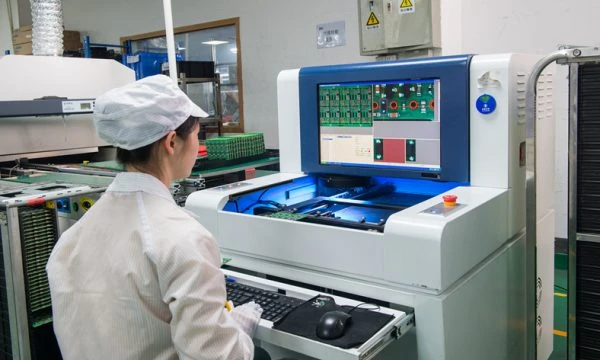
When to use ICT (In-Circuit Test)
- High Volume Production: The speed of ICT (often 10–30 seconds per panel) justifies the high initial fixture cost.
- Mature Designs: If the PCB layout is stable, the fixture investment is safe. Frequent layout changes render ICT fixtures obsolete.
- Component-Level Diagnostics: You need to know exactly which resistor is the wrong value or which pin is unsoldered for immediate rework.
- Power-Off Testing: You want to check for shorts before applying power to prevent catastrophic board damage.
- DFT Compliance: Your board has accessible test points (pads) for at least 90% of the nets.
When to use FCT (Functional Circuit Test)
- Functional Verification: You must prove the device boots, communicates via UART/USB, or drives a motor.
- Low to Medium Volume: If producing fewer than 500–1,000 units, the setup cost of a complex ICT fixture may not be amortizable.
- Final Quality Gate: This is the "does it work?" test before shipping to the customer.
- Firmware Validation: You need to verify that the microcontroller is programmed correctly and executing code.
- Limited Access: The PCB is too dense for a bed-of-nails fixture, or you can only access edge connectors.
Rules & specifications
The following table outlines the technical specifications and decision rules for selecting the correct testing strategy. These parameters help engineers quantify the trade-offs in ict test vs fct test: when to use which.
| Rule | Recommended Value/Range | Why it matters | How to verify | If ignored |
|---|---|---|---|---|
| Production Volume Threshold | ICT: >1,000 units/run FCT: Any volume |
Amortizes the high cost of ICT fixtures ($2k–$15k) over many units. | Check BOM quantity and annual forecast. | ROI is negative; unit cost increases significantly due to fixture NRE. |
| Test Point Diameter (ICT) | Min 0.8mm (ideal), 0.5mm (limit) | Ensures pogo pins hit the target reliably without slipping. | Review Gerber files in a Gerber Viewer. | High false failure rate; pins damage the PCB mask or copper. |
| Test Point Spacing (ICT) | Center-to-center: 2.54mm (standard), 1.27mm (min) | Prevents shorting between probes and allows standard probes. | Measure distance in CAD layout tools. | Requires expensive specialized probes; increases fixture cost. |
| Fault Coverage Target | ICT: 90–95% (Mfg defects) FCT: 100% (Function) |
ICT catches shorts/opens; FCT catches logic errors. | Review Test Coverage Report from CAM engineer. | Escaped defects reach the field; high RMA rates. |
| Cycle Time per Unit | ICT: 10–60 sec FCT: 1–10 min |
Determines line throughput and daily output capacity. | Simulate test steps; stopwatch timing on prototype. | Production bottlenecks; missed delivery deadlines. |
| Voltage Levels | ICT: Low voltage (<12V) FCT: Operating voltage |
ICT is mostly passive/low power; FCT uses real power. | Check schematic power rails. | ICT probes may arc if high voltage is applied incorrectly. |
| Fixture Lead Time | ICT: 2–4 weeks FCT: 1–3 weeks |
Affects time-to-market for the first production batch. | Confirm with APTPCB (APTPCB PCB Factory) engineering team. | Production delays waiting for tooling. |
| Diagnostic Granularity | ICT: Pin-level FCT: Block-level |
ICT tells you "R45 is open". FCT says "Output is 0V". | Review failure report format requirements. | Troubleshooting FCT failures takes hours instead of minutes. |
| Firmware Dependency | ICT: None (usually) FCT: Required |
FCT requires stable firmware to run the test routine. | Check firmware release schedule. | FCT cannot proceed if firmware is buggy or unavailable. |
| Board Strain | Max 500 microstrain | ICT fixtures apply pressure; excessive bending breaks solder joints. | Strain gauge analysis during fixture commissioning. | Micro-cracks in MLCC capacitors; latent field failures. |
Implementation steps
Once you have analyzed the rules, follow this process to implement the chosen strategy. This workflow ensures that whether you choose ICT, FCT, or both, the integration into the manufacturing line at APTPCB is seamless.
Define Defect Spectrum
- Action: List the most likely failure modes (e.g., BGA soldering, wrong resistor value, firmware corruption).
- Parameter: Defect Parts Per Million (DPPM) target.
- Check: If soldering defects are the main concern, prioritize ICT or AOI. If logic is key, prioritize FCT.
Design for Test (DFT) Review
- Action: Analyze the PCB layout for test point accessibility.
- Parameter: Test point density > 90% net coverage for ICT.
- Check: Use DFM Guidelines to ensure test points are not covered by solder mask.
Select Fixture Type
- Action: Choose between Clamshell (dual-sided) or Vacuum (single-sided) for ICT; or a custom jig for FCT.
- Parameter: Mechanical clearance (component height).
- Check: Ensure tall capacitors do not interfere with the press-down mechanism.
Generate Test Program
- Action: For ICT, export CAD data (ODB++ or IPC-356). For FCT, write the test script (Python/LabVIEW).
- Parameter: Netlist integrity.
- Check: Verify the netlist matches the schematic exactly to avoid false shorts.
Fabricate and Debug Fixture
- Action: Machine the fixture and wire the probes. Run "Golden Sample" boards.
- Parameter: Cpk (Process Capability) > 1.33 for analog measurements.
- Check: Repeatedly test a known good board 50 times to ensure zero false failures.
Integrate into Production Line
- Action: Place the station after reflow (for ICT) or after assembly (for FCT).
- Parameter: Takt time matching.
- Check: Ensure the test station does not become the bottleneck of the assembly line.
Validation and Sign-off
- Action: Run a pilot lot (e.g., 50 units).
- Parameter: First Pass Yield (FPY).
- Check: If FPY < 95%, pause and adjust limits or fixture mechanics.
Failure modes & troubleshooting
Even with a robust strategy for ict test vs fct test: when to use which, issues arise during execution. Troubleshooting requires distinguishing between a bad board and a bad test setup.
Symptom: High False Failure Rate (ICT)
- Causes: Flux residue on test points, worn pogo pins, board warping.
- Checks: Inspect test pads for contamination; measure probe resistance.
- Fix: Clean test points; replace pogo pins; adjust hold-down pins.
- Prevention: Implement a cleaning cycle for probes every 1,000 cycles.
Symptom: Board Passes FCT but Fails in Field
- Causes: Marginal design (timing/voltage), test limits too loose, intermittent solder joints not stressed.
- Checks: Review FCT test limits against datasheet max/min; check if vibration/thermal stress is needed.
- Fix: Tighten pass/fail limits; add "corner case" tests (min/max voltage).
- Prevention: Perform Design Verification Testing (DVT) before finalizing FCT specs.
Symptom: Pogo Pin Damage to PCB Pads
- Causes: Excessive spring force, sharp probe tips, misalignment.
- Checks: Microscope inspection of test pads after testing.
- Fix: Switch to crown or cup style tips; reduce spring force.
- Prevention: Specify "witness mark" limits in the fixture design document.
Symptom: FCT Station Bottleneck
- Causes: Test routine too long, slow boot time, manual operator steps.
- Checks: Profile the test script execution time.
- Fix: Parallelize tests (multi-up fixture); optimize boot sequence; automate connector insertion.
- Prevention: Calculate cycle time during the PCB Manufacturing planning phase.
Symptom: Phantom Shorts (ICT)
- Causes: Large capacitors discharging, guarding errors, moisture.
- Checks: Verify discharge delay settings; check humidity levels.
- Fix: Add "Wait" commands before measurement; improve guarding techniques.
- Prevention: Ensure proper board cleaning and drying before testing.
Symptom: Inconsistent Analog Readings
- Causes: Ground loops, noise in fixture wiring, poor contact.
- Checks: Measure ground resistance between DUT and tester.
- Fix: Use twisted pair wiring in fixture; implement differential measurements.
- Prevention: Design fixture with dedicated ground planes and shielding.
Design decisions
Making the final call on ict test vs fct test: when to use which often involves balancing engineering constraints with business goals.
The "Coverage vs. Cost" Trade-off
ICT provides excellent coverage for manufacturing process defects (solder bridges, missing parts) but tells you nothing about whether the design works. FCT proves the design works but might miss a latent solder defect that only fails later.
- Decision: For consumer electronics with short lifecycles, FCT alone might suffice. For industrial controls, APTPCB recommends both.
Test Point Strategy
If you choose ICT, you must commit to it during the layout phase.
- Constraint: Adding test points takes up board space and affects signal integrity on high-speed lines.
- Decision: If the board is extremely dense (e.g., smartphone mainboard), traditional ICT is impossible. Use Flying Probe (for prototypes) or rely on FCT + AOI (Automated Optical Inspection).
Data Logging and Traceability
- Requirement: Automotive and medical clients often require individual test results stored by serial number.
- Decision: ICT systems naturally output detailed logs. FCT systems often require custom software development to save logs to a database. Ensure your FCT setup includes a barcode scanner and database integration.
FAQ
1. Can I replace ICT with AOI (Automated Optical Inspection)? AOI checks for visual defects (presence, polarity, solder quality) but cannot verify electrical values or hidden solder joints (like BGAs). ICT is electrically superior but AOI is non-contact and fixture-free. They complement each other.
2. Is FCT mandatory if I do ICT? Not always, but highly recommended. ICT confirms the board was built correctly; FCT confirms it functions correctly. Skipping FCT risks shipping boards with bad firmware or timing issues.
3. What is the typical cost difference between ICT and FCT fixtures? ICT fixtures (Bed of Nails) typically cost between $2,000 and $15,000 depending on point count. FCT fixtures can be cheaper ($500–$5,000) if simple, or very expensive if they require complex automation and RF shielding.
4. How do I design test points for ICT on dense PCBs? Use smaller test pads (0.5mm) and stagger them. If density is too high, target only critical nets (power, ground, data buses) and rely on Boundary Scan (JTAG) for digital logic testing.
5. Can one fixture do both ICT and FCT? Yes, these are called "Functional Bed of Nails" fixtures. They use pogo pins to access the board but run functional tests. However, signal integrity can be an issue due to the long wires in the fixture.
6. What is a "Flying Probe" test? Flying probe is a fixtureless ICT. Robotic arms move probes to test points. It is very slow (minutes per board) but has zero fixture cost. It is ideal for prototypes, while bed-of-nails ICT is for mass production.
7. Does APTPCB handle fixture fabrication? Yes, we coordinate the design and fabrication of test fixtures as part of our turnkey assembly services.
8. How does firmware flashing fit into this? Firmware is usually flashed before FCT. Some ICT testers can flash small firmware files, but it is slow. Dedicated gang programmers or FCT stations are better for flashing.
9. What if my board has no space for test points? You may be limited to FCT via edge connectors and AOI/X-Ray for process verification. This increases the risk of difficult troubleshooting if a board fails.
10. How long does it take to develop an FCT test? It depends on complexity. A simple power-up test takes 1–2 days. A full functional suite with software development can take 2–4 weeks.
11. What is "Test Coverage"? It is the percentage of potential defects that a test method can detect. ICT typically covers 90%+ of shorts/opens. FCT covers functional blocks but has low structural coverage.
12. Can I use JTAG instead of ICT? Boundary Scan (JTAG) can test digital interconnections without physical test points. It is a powerful alternative to ICT for digital sections but cannot test analog components or power rails effectively.
Glossary (key terms)
| Term | Definition | Context |
|---|---|---|
| ICT (In-Circuit Test) | Testing individual components and connections on a PCB using a bed-of-nails fixture. | Manufacturing Defect Analysis. |
| FCT (Functional Circuit Test) | Testing the PCB as a complete system to verify it performs its intended function. | Final Quality Control. |
| Bed of Nails | A fixture containing spring-loaded pins (pogo pins) that make contact with test points on the PCB. | ICT Hardware. |
| Pogo Pin | A spring-loaded probe used to establish electrical contact between the tester and the DUT. | Fixture Component. |
| DUT (Device Under Test) | The PCB or assembly currently being tested. | General Testing. |
| DFT (Design for Test) | Designing a PCB layout specifically to make testing easier (e.g., adding test points). | PCB Design Phase. |
| AOI (Automated Optical Inspection) | Using cameras to visually inspect solder joints and component placement. | Pre-ICT Inspection. |
| NRE (Non-Recurring Engineering) | One-time costs for research, design, and tooling (like fixtures). | Cost Analysis. |
| False Fail | A test result indicating a defect when the board is actually good (often due to fixture issues). | Troubleshooting. |
| Golden Sample | A known good board used to calibrate and verify the test fixture. | Setup & Validation. |
| Boundary Scan (JTAG) | A method to test interconnects between ICs without physical probes using the JTAG interface. | Digital Testing. |
| FPY (First Pass Yield) | The percentage of boards that pass testing on the first attempt without rework. | Quality Metric. |
Conclusion
Choosing between ict test vs fct test: when to use which is not a binary choice but a strategic one based on volume and quality goals. ICT offers speed and precise diagnostics for mass production, while FCT ensures the final product actually works for the end-user. For most high-quality electronics, a combination of AOI, ICT, and FCT provides the highest assurance.
At APTPCB, we help you optimize this strategy from the design phase through to final assembly. By planning your test points early and selecting the right fixture, you reduce lead times and ensure zero-defect delivery.
Ready to finalize your test strategy? Submit your design for a Quote and let our engineers review your DFT requirements today.