
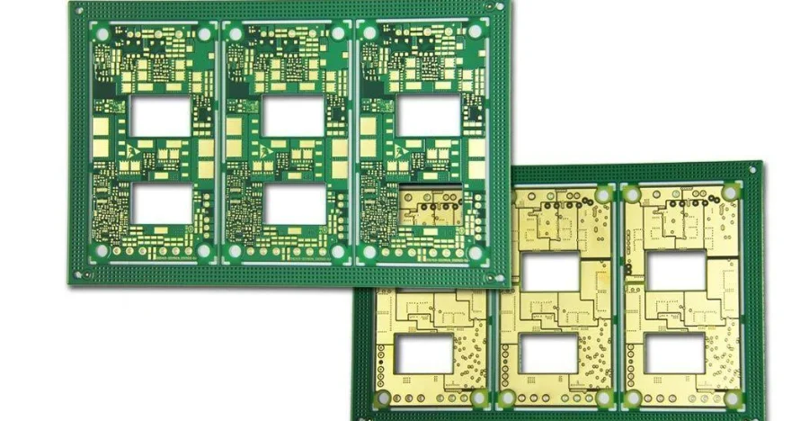
Designing a medical PCB for IEC 60601-1 compliance requires more than placing a large gap between primary and patient-side circuits. The isolation boundary must survive the complete product lifecycle: schematic definition, PCB layout, fabrication, assembly, inspection, and final medical-device qualification.
Direct answer: For a commonly referenced 250VAC working voltage with 2 MOPP patient protection, engineers often work with a design target of 8.0mm creepage distance, 5.0mm clearance distance, and a 4000VAC dielectric withstand requirement. These values describe a safety design condition, not a universal PCB rule. The final requirement depends on the medical device architecture, insulation classification, working voltage, and applicable IEC 60601-1 interpretation.
What is IEC 60601-1?
IEC 60601-1 is the international basic safety and essential performance standard for medical electrical equipment, published in Europe as EN 60601-1 (and adopted nationally, for example as CEI EN 60601-1 in Italy). Particular standards in the IEC 60601-2-x series add requirements for specific device types. For the PCB, the parts that matter most are the insulation rules (creepage, clearance, dielectric strength) and the leakage current limits.
A successful design converts the safety analysis into measurable PCB requirements:
- define the isolation boundary;
- reserve physical spacing across every PCB layer;
- control copper, vias, pads, and mechanical features;
- specify materials and manufacturing controls;
- verify that the fabricated PCB matches the approved construction.
What are IEC 60601-1 creepage and clearance requirements for 2 MOPP PCB designs?
IEC 60601-1 separates operator protection and patient protection because patient-connected circuits require stricter safeguards.
- MOOP (Means of Operator Protection) applies to protection of operators and accessible users.
- MOPP (Means of Patient Protection) applies to circuits that may connect directly or indirectly to patients.
A 2 MOPP barrier represents two independent means of patient protection. For a typical 250VAC condition, a frequently referenced design requirement is:
| Protection Requirement | Working Voltage | Creepage | Clearance | Dielectric Withstand Reference |
|---|---|---|---|---|
| 1 MOPP | 250VAC | 4.0mm | 2.5mm | 1500VAC |
| 2 MOPP | 250VAC | 8.0mm | 5.0mm | 4000VAC |
Patient leakage current limits (Patientenableitstrom)
Spacing is only half of the patient-protection requirement. IEC 60601-1 also limits the leakage current that may flow through the patient, depending on the applied-part type. The commonly cited normal-condition patient leakage limits are:
| Applied part type | Typical use | Patient leakage current, normal condition (AC) |
|---|---|---|
| Type B | No conductive patient contact, or non-cardiac contact | 100 µA |
| Type BF | Floating applied part with body contact | 100 µA |
| Type CF | Direct cardiac application | 10 µA |
Single-fault limits are higher, and DC limits are lower. Take the full table from the edition of the standard named in the risk file. On the PCB, leakage is driven by the isolation barrier's capacitance (isolated DC/DC converters, Y-capacitors and optocouplers) as much as by spacing, so BF and CF designs often need low-capacitance isolation components.
The values above should be confirmed against the applicable safety analysis. The PCB designer should not assume that changing laminate material or adding coating automatically changes the required spacing.
What design information should be defined before PCB layout?
A medical PCB isolation boundary begins with system-level decisions.
| Design Input | Engineering Impact | RFQ Requirement |
|---|---|---|
| Working voltage | Determines electrical stress across the barrier | Document maximum operating condition |
| Protection level | Defines required insulation strength | Specify 1 MOPP, 2 MOPP, MOOP, or equivalent requirement |
| Applied-part classification | Changes patient-side risk assumptions | Identify patient-connected nets |
| Pollution environment | Influences insulation performance considerations | Confirm operating environment |
| Material requirement | May affect creepage calculation | Specify laminate grade and CTI requirement |
| Test voltage | Defines dielectric verification | State test boundary and responsibility |
| Manufacturing tolerance | Changes final isolation distance | Include finished dimension requirements |
The most important step is creating a controlled isolation boundary that can be reviewed by both safety engineers and PCB manufacturers.
How should a PCB layout achieve 2 MOPP isolation?
The isolation boundary must exist through the complete PCB structure, not only on the top copper layer.
A production-ready layout should consider:
- top-layer traces;
- bottom-layer copper;
- internal power and ground planes;
- plated through holes;
- component pads;
- connector pins;
- mounting hardware;
- solder mask openings;
- PCB edges;
- assembly tolerances.
A typical isolation workflow is:
- Create a dedicated PCB isolation keepout.
- Remove copper from every affected layer.
- Check all vias and component footprints near the barrier.
- Confirm mechanical dimensions after fabrication tolerance.
- Release manufacturing drawings that describe critical isolation features.
Standard spacing rules used for signal routing are not sufficient. Safety isolation requires dedicated design rules. On a multilayer PCB, the keepout has to be checked on every inner layer as well, and the dielectric between layers across the barrier becomes part of the insulation system (distance through insulation). The same reasoning applies to any high voltage PCB design that carries a reinforced barrier.
What PCB design options solve limited-space isolation problems?
Medical products often need smaller boards while maintaining large isolation distances. Engineers typically evaluate spacing, slots, materials, and coatings.
| Solution | Engineering Benefit | Main Consideration |
|---|---|---|
| Increased PCB spacing | Simple and predictable isolation method | Requires sufficient board area |
| High-CTI laminate | Can improve material classification where applicable | Does not automatically reduce 2 MOPP spacing |
| Isolation slots | Extends surface creepage path | Requires controlled mechanical dimensions |
| Conformal coating | Adds environmental protection | Cannot automatically replace required spacing |
The correct choice depends on the approved insulation system.
Can high-CTI PCB material reduce IEC 60601 creepage distance?
High-CTI materials can improve tracking resistance and may influence creepage calculations in standards where material group is considered.
However, high CTI does not create a general exemption from medical isolation spacing requirements.
For example, a PCB specification may require:
- CTI value;
- material group;
- laminate manufacturer;
- dielectric thickness;
- approved substitutions.
A procurement document that only states “FR-4” does not provide enough control for a safety-critical medical PCB.
When the design depends on high-CTI material, specify the required property directly, such as CTI > 600V / PLC 0, and require supplier confirmation.
When do PCB isolation slots improve creepage performance?
Isolation slots are frequently used when the PCB footprint cannot provide a straight surface path.
A slot can force the creepage route around the opening, increasing the effective surface distance between conductive regions.
A production slot specification should include:
- finished slot width;
- finished slot length;
- copper-to-slot clearance;
- plated or non-plated construction;
- routing tolerance;
- nearby component restrictions.
The slot must be evaluated as part of the insulation system. A narrow opening does not automatically convert a creepage requirement into a clearance requirement.
What causes IEC 60601 PCB isolation failures?
A PCB can pass design review and still fail electrical testing because the real manufactured structure differs from the assumed model.
| Failure Mode | Root Cause | Verification Method |
|---|---|---|
| Insufficient creepage | Copper, pads, or contamination shorten surface path | Layout review and inspection |
| Insufficient clearance | Components or hardware reduce air gap | Mechanical inspection |
| Internal plane intrusion | Copper extends into isolation region | CAM verification |
| Wrong laminate | Material does not match approved insulation system | Material certification |
| Surface tracking | Flux residue or contamination creates leakage path | Cleanliness testing |
| Dielectric breakdown | Stackup or insulation thickness failure | Electrical-strength testing |
Hi-Pot testing and dimensional inspection verify different characteristics.
A board can have correct spacing but fail dielectric testing.
A board can pass Hi-Pot testing but still contain an incorrect creepage path.
Both verification methods are required when defined by the project qualification plan.
What validation evidence should a medical PCB supplier provide?
A medical PCB supplier should provide evidence that the manufactured board matches the approved design.
| Requirement | Supplier Evidence |
|---|---|
| Isolation geometry | Dimensional inspection records |
| Material compliance | Laminate identification and certificates |
| Stackup control | Stackup report and microsection when required |
| Clean manufacturing | Ionic contamination data where specified |
| Slot accuracy | Mechanical inspection results |
| Electrical verification | Defined dielectric test records |
Manufacturing verification supports medical-device compliance, but PCB fabrication alone does not certify the complete medical product. Bare-board evidence normally comes from the fabricator's PCB quality and inspection records, and assembly evidence from the assembler's process records. For a worked example of a patient-connected power stage, see the life support power PCB isolation guide.
The medical-device manufacturer remains responsible for IEC 60601-1 system qualification.
What should be included in a medical PCB RFQ?
A strong RFQ prevents safety-critical assumptions from being lost during supplier communication.
Include:
- required MOP classification;
- working voltage;
- minimum creepage distance;
- minimum clearance distance;
- insulation boundary drawings;
- approved laminate requirements;
- CTI requirements;
- stackup restrictions;
- slot dimensions;
- cleanliness requirements;
- inspection requirements;
- electrical test expectations;
- engineering-change approval process.
A supplier comparison should evaluate not only price and lead time but also the ability to maintain safety-critical geometry. Our medical PCB manufacturing page lists the documentation and traceability APTPCB provides for medical programs. When assembly is included, medical PCBA assembly under a turnkey order keeps component lots, cleanliness data and Hi-Pot records together.
Medical PCB supplier decision checklist
Before production release, confirm:
| Supplier Capability | Confirmation |
|---|---|
| Can maintain required creepage and clearance? | Confirm with fabrication review |
| Can control isolation slots? | Confirm mechanical tolerance capability |
| Can provide material traceability? | Request documentation |
| Can verify stackup construction? | Request inspection capability |
| Can support cleanliness requirements? | Confirm process controls |
| Can manage engineering changes? | Establish approval workflow |
The most reliable IEC 60601-1 PCB projects treat isolation as a controlled manufacturing requirement, not only a layout rule.
For a 250VAC 2 MOPP boundary, the commonly referenced design targets of 8.0mm creepage, 5.0mm clearance, and 4000VAC dielectric-strength verification should be carried from the safety analysis into PCB layout rules, fabrication drawings, inspection plans, and supplier documentation.
That connection between engineering intent and manufacturing evidence is what turns a medical PCB design into a production-ready safety component.