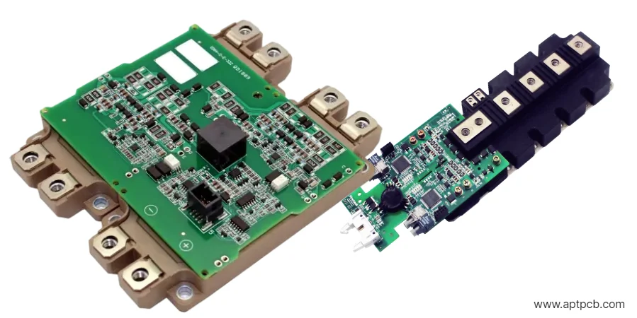
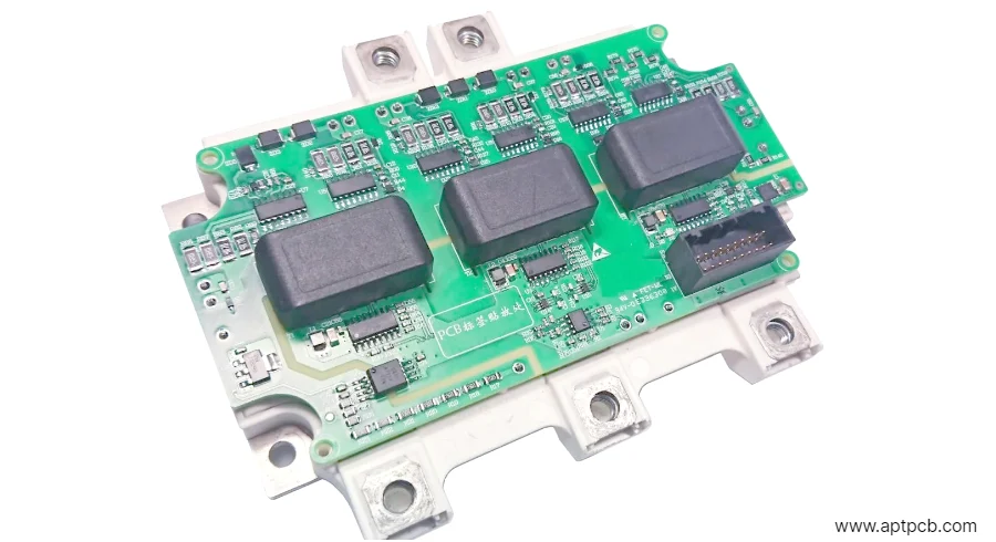
IGBT gate driver assemblies control insulated gate bipolar transistors handling multi-kilowatt to megawatt power levels requiring precise gate charge control, desaturation protection, and optimized switching trajectories achieving sub-1% total losses while preventing failures from shoot-through, overcurrent, or thermal stress across industrial motor drives, railway traction inverters, and utility-scale power conversion operating continuously through millions of switching cycles over 20-30 year service lives.
At APTPCB, we deliver specialized IGBT driver assembly services with PCB stencil precision implementing protection circuits, active gate control, and robust isolation. Our capabilities support IGBT modules from 200A through 3600A across voltage ratings from 600V industrial drives through 6500V medium-voltage applications with comprehensive functional testing.
Optimizing IGBT Turn-On and Turn-Off
IGBT switching optimization requires balancing multiple competing requirements: fast turn-on minimizes switching losses but increases dv/dt stress on motor insulation; slow turn-off reduces tail current losses but extends switching time increasing total losses; excessive gate current causes overshoot and ringing while insufficient current extends dead-time increasing body diode conduction losses. Proper optimization achieves <1% switching losses while maintaining EMI compliance and reliable operation.
At APTPCB, our assembly services implement optimized gate drive circuits achieving specified switching performance.
Key Switching Optimization Techniques
Turn-On Control
- Two-stage turn-on using initial slow gate charging controlling di/dt followed by fast charging minimizing conduction time with turnkey assembly integrating discrete or IC-based drive circuits
- Gate resistance selection (typically 1-10Ω) balancing turn-on speed against voltage overshoot from stray inductance
- Soft turn-on limiting initial di/dt preventing high reverse recovery current in freewheeling diodes reducing losses and EMI
- Active gate drive adjusting gate current dynamically based on collector current or operating conditions
- Temperature compensation maintaining consistent switching despite gate threshold voltage shifts with temperature
- Testing quality validation measuring turn-on waveforms across production units ensuring consistency
Turn-Off Optimization
- Controlled turn-off managing current fall time and voltage rise time independently optimizing losses
- Two-stage turn-off using initial fast discharge reducing conduction time followed by controlled discharge managing dv/dt
- Active clamping during turn-off limiting voltage overshoot from stray inductance protecting IGBT while minimizing snubber losses
- Tail current management using negative gate voltage (-5 to -15V) accelerating carrier removal reducing tail current duration
- Load current dependent optimization adjusting turn-off speed based on current level balancing losses and stress
- Comprehensive functional testing validating turn-off performance across current and temperature ranges
Gate Resistance Design
- Separate turn-on and turn-off resistors independently optimizing each transition
- Parallel resistor configurations enabling multi-stage switching trajectories
- Series inductance in gate circuit providing additional control of di/dt and dv/dt
- Temperature-stable resistors maintaining characteristics across operating temperatures
- Power rating adequate for high-frequency ripple current dissipation
- Precision tolerance resistors (±1%) ensuring consistent switching across parallel IGBTs
Implementing Desaturation Protection
Desaturation (DESAT) protection detects short circuits or overcurrent by monitoring collector-emitter voltage during on-state. Normal saturation voltage (Vce(sat)) ranges 1.5-3V depending on current, but short circuit causes voltage to rise toward DC bus within microseconds requiring fast detection (<2μs) and shutdown preventing thermal destruction. DESAT circuits must provide blanking during turn-on, avoid false trips from normal operation, and coordinate with system protection.
APTPCB implements validated DESAT circuits ensuring reliable short circuit protection.
Key DESAT Implementation
Detection Circuit Design
- High-voltage diode string isolating sense circuit from high collector voltage
- Comparator detecting voltage rise above threshold (typically 7-10V) indicating desaturation
- Blanking circuit disabling detection during turn-on ignoring high voltage during normal switching
- Filtering preventing false triggers from noise or switching transients
- Fast response (<1μs) triggering soft turn-off before thermal damage
- Quality system controls ensuring DESAT circuit consistency across production
Blanking Time Optimization
- Turn-on blanking (typically 2-8μs) allowing IGBT to enter saturation before enabling detection
- Current-dependent blanking accommodating longer saturation times at heavy loads
- Temperature-compensated blanking accounting for slower switching at temperature extremes
- Trade-off between detection speed and false trip prevention
- Validation testing at boundary conditions ensuring reliable detection without false trips
- NPI assembly prototyping enabling DESAT circuit optimization before production
Fault Response
- Soft turn-off controlling gate discharge preventing voltage overshoot from rapidly collapsing collector current
- Fault latch holding gate off until system reset preventing repeated fault attempts
- Status reporting communicating fault to system controller enabling coordinated shutdown
- Diagnostic information capturing fault conditions supporting troubleshooting and analysis
- Recovery timing coordinating with system protection preventing unsafe restart attempts
- Multi-layer protection combining DESAT with overcurrent sensing providing redundancy
Managing Miller Effect and Parasitic Turn-On
Miller effect creates unwanted gate charge/discharge through gate-collector capacitance during voltage transitions potentially causing parasitic turn-on or slowed switching. During dv/dt transients when opposite IGBT turns on, Miller current flows through gate-collector capacitance potentially charging gate above threshold causing shoot-through. Active Miller clamp circuits prevent parasitic turn-on maintaining gate below threshold despite high dv/dt.
APTPCB implements comprehensive Miller effect management ensuring reliable switching.
Key Miller Effect Mitigation
Active Miller Clamp
- Low-impedance gate discharge path activated during off-state maintaining gate voltage below threshold
- Clamp activation during high dv/dt preventing Miller current from raising gate voltage
- Separate clamp circuits for turn-on and turn-off optimizing each transition independently
- Proper timing ensuring clamp doesn't interfere with intentional gate drive signals
- Component selection providing adequate current sinking capability handling peak Miller current
- Mass production assembly ensuring consistent clamp circuit performance
Negative Gate Voltage
- Negative supply (-5 to -15V) pulling gate below threshold providing immunity to Miller effect
- Enhanced turn-off using negative voltage accelerating gate discharge and carrier removal
- Reduced tail current from faster carrier extraction improving efficiency
- Isolated negative supply generation using charge pumps or isolated DC-DC converters
- Supply sequencing ensuring negative supply available before enabling switching
- Testing validation across operating conditions confirming parasitic turn-on immunity
Providing Isolated Power and Signals
IGBT modules in three-phase inverters require six isolated gate driver supplies powering high-side and low-side drivers. Each driver requires 15-20V positive supply, optional negative supply, and signal isolation maintaining barriers despite common-mode transients exceeding 50kV/μs. Power isolation implementation influences system cost, efficiency, reliability, and electromagnetic compatibility requiring careful architecture selection.
APTPCB assembles gate driver boards with validated isolation strategies.
Key Isolation Implementation
Isolated Power Architectures
- Transformer-isolated DC-DC converters providing independent supplies to each gate driver
- Isolated gate driver ICs integrating power and signal isolation in single package
- Capacitive power transfer using coreless transformer technology
- Bootstrap supplies for high-side drivers in cost-sensitive applications
- Supply redundancy and monitoring ensuring continued operation despite single failure
- Component sourcing managing specialized isolation components and transformers
Signal Isolation Methods
- Fiber optic isolation immune to electromagnetic interference in hostile electrical environments
- High-speed digital isolators (>100Mbps) transmitting PWM signals with minimal propagation delay
- Matched propagation delays between phases preventing timing skew causing circulating currents
- Common-mode transient immunity (CMTI) >50kV/μs surviving fast voltage transitions during switching
- Robust PCB layout maintaining isolation integrity despite contamination or moisture
- PCB conformal coating protecting isolation barriers from environmental exposure
Ensuring Thermal Management
Gate driver circuits dissipate power from gate charge/discharge, quiescent current in driver ICs, and resistive losses in gate resistors. At 20kHz switching frequency with 200nC gate charge and 15V supply, gate drive power reaches 60mW per IGBT—minor compared to IGBT losses but significant for driver IC junction temperatures. Inadequate thermal management causes driver overheating reducing reliability or triggering thermal shutdown interrupting operation.
APTPCB implements thermal design ensuring reliable driver operation.
Key Thermal Design Requirements
Heat Dissipation Strategy
- Proper copper pour beneath driver ICs and gate resistors spreading heat
- Thermal vias transferring heat through PCB to heat sink or opposite side
- Component spacing maintaining adequate clearance preventing thermal coupling
- Heat sink integration when required for high-frequency or high-power applications
- Thermal simulation validating junction temperatures remain within specifications
- Special PCB manufacturing using high thermal conductivity materials when needed
Component Selection
- Driver ICs with adequate power rating and thermal shutdown protection
- Gate resistors rated for ripple current and power dissipation
- Isolated supplies with thermal derating considered in power budget
- Temperature sensors monitoring critical areas enabling thermal management
- Extended temperature range components surviving automotive or industrial environments
- Production testing validating thermal performance under worst-case conditions
Supporting Industrial and Traction Applications
IGBT gate drivers serve demanding applications including industrial motor drives (cement mills, mining conveyors, compressors), railway traction (locomotives, metros, tramways), and utility infrastructure (HVDC, STATCOM, SVCs) requiring ruggedized construction, extended qualification testing, and long service life. Application-specific requirements influence design choices, component selection, and certification strategies necessitating flexible manufacturing and engineering support.
APTPCB supports diverse IGBT applications with application-optimized manufacturing.
Key Application Requirements
Industrial Motor Drives
- 4-8kHz switching optimizing motor performance and acoustic noise
- Multi-level topologies (NPC, ANPC, flying capacitor) reducing dv/dt stress
- Harsh environment ratings surviving factory floor dust, humidity, and temperature
- 20+ year design life matching industrial equipment expectations
- Certifications (UL, CE, CCC) enabling global market access
- Communication interfaces (Modbus, Profinet) integrating into factory automation
Railway Traction Systems
- Extreme reliability requirements (>25 years) withstanding vibration, shock, and thermal cycling
- EN 50155 railway electronics standard compliance
- Wide temperature range (-40 to +85°C) surviving diverse climates globally
- Galvanic isolation (4-6kV) ensuring passenger safety
- EMC compliance in electromagnetically harsh railway environment
- Maintainability supporting depot-level repair and diagnostics
Through application-specific optimization, robust manufacturing processes, and comprehensive qualification testing, APTPCB enables IGBT applications across industrial, transportation, and utility markets requiring reliable multi-kilowatt to megawatt power conversion.