Quick Answer (30 seconds)
High-performance Imaging Radar PCB fabrication requires strict control over material dielectric properties and etching precision to support high-resolution 4D sensing.
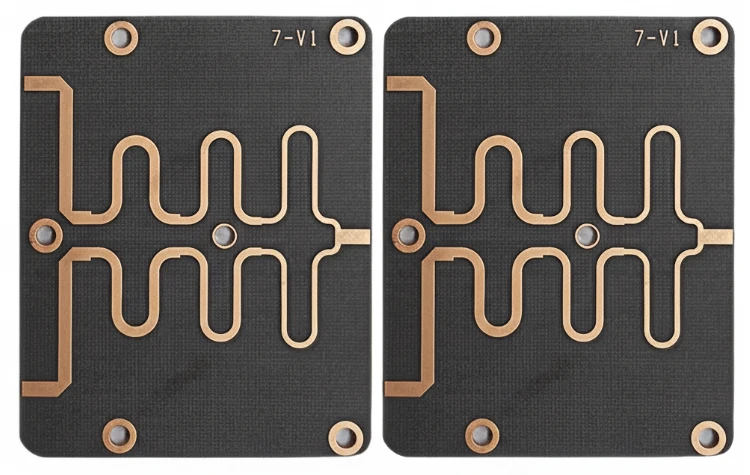
- Material Choice: Use low-loss laminates (Df < 0.003) like Rogers RO3003 or Panasonic Megtron 7 for the antenna layer.
- Frequency Range: Most imaging radars operate at 77GHz or 79GHz; standard FR4 is unusable for these RF layers due to high signal attenuation.
- Etching Precision: Antenna patch dimensions typically require ±15µm or tighter tolerance to ensure accurate phase information.
- Stackup Strategy: Hybrid stackups (High-frequency material + FR4) are standard to balance signal integrity with mechanical rigidity and cost.
- Surface Finish: Immersion Silver or ENEPIG is preferred; HASL is prohibited due to uneven surfaces affecting antenna gain.
- Validation: 100% Automated Optical Inspection (AOI) and insertion loss testing are mandatory before final assembly.
When Imaging Radar PCB applies (and when it doesn’t)
Imaging radar technology bridges the gap between standard radar and LiDAR, offering high resolution in point clouds. Knowing when to deploy a specialized Imaging Radar PCB versus a standard radar board is critical for cost and performance.
Use Imaging Radar PCB when:
- High Angular Resolution is required: You need less than 1° angular resolution to distinguish static objects (guardrails) from moving objects (pedestrians).
- Elevation Sensing is needed: The application requires "4D" data (Range, Doppler, Azimuth, and Elevation), typical in 4D Radar PCB designs.
- Operating at Millimeter Wave: The system uses 77GHz Radar PCB or 79GHz Radar PCB bands where skin depth and dielectric loss are critical factors.
- Complex MIMO Arrays: The design involves large Multiple-Input Multiple-Output (MIMO) antenna arrays (e.g., 48 Tx / 48 Rx) requiring precise phase matching.
- Safety-Critical ADAS: Used in Level 3+ autonomous driving where sensor fusion reliability is non-negotiable.
Do not use Imaging Radar PCB when:
- Simple Proximity Sensing: Basic blind-spot detection or parking assist often uses simpler 24GHz Radar PCB designs on cheaper substrates.
- Low Data Rate Applications: If the system only detects "presence" rather than "object classification," standard RF materials may suffice.
- Cost-Sensitive Consumer Toys: High-frequency laminates are expensive; standard FR4 is better for non-critical drone toys or automatic door openers.
- Low Frequency Operation: Sub-6GHz applications do not require the extreme etching tolerances and expensive PTFE/ceramic materials of imaging radar.
Rules & specifications
To achieve the signal clarity required for imaging, the PCB fabrication process must adhere to tighter tolerances than standard IPC Class 2 boards. APTPCB (APTPCB PCB Factory) recommends the following specifications for optimal yield and performance.
| Rule | Recommended value/range | Why it matters | How to verify | If ignored |
|---|---|---|---|---|
| Line Width Tolerance | ±10µm to ±15µm | Directly impacts impedance and antenna resonance frequency. | AOI (Automated Optical Inspection) | Frequency shift; reduced detection range. |
| Dielectric Thickness | ±5% or tighter | Controls impedance and phase velocity of the radar signal. | Microsection analysis | Impedance mismatch; signal reflection. |
| Copper Roughness | VLP or HVLP (< 1µm Rz) | Reduces conductor loss due to skin effect at 77GHz. | SEM (Scanning Electron Microscope) | High insertion loss; reduced signal-to-noise ratio. |
| Registration Accuracy | ±3 mil (75µm) | Ensures alignment between antenna patches and feed lines on different layers. | X-Ray drill verification | Phase errors; degraded beamforming capability. |
| Surface Finish | Immersion Silver / ENEPIG | Provides a flat surface for antenna patches; minimizes skin effect losses. | XRF thickness measurement | Signal attenuation; soldering defects on BGA. |
| Solder Mask Opening | +2 mil (50µm) over pad | Prevents mask from encroaching on antenna elements (mask alters Dk). | Visual inspection / AOI | Detuning of antenna elements. |
| Via Aspect Ratio | 8:1 to 10:1 | Ensures reliable plating in through-holes for grounding and thermal paths. | Cross-section analysis | Open circuits; thermal failure of MMIC. |
| Dk Tolerance | ±0.05 | Consistent dielectric constant is vital for phase accuracy in MIMO arrays. | IPC-TM-650 test methods | Beam squinting; inaccurate object location. |
| Bow and Twist | < 0.5% | Critical for BGA assembly of large radar chipsets. | Flatness gauge | Assembly failure; stress on solder joints. |
| Cleanliness | Ionic contamination < 1.0 µg/cm² | Prevents electrochemical migration in harsh automotive environments. | Rose Test / Ion Chromatography | Field failure due to corrosion or leakage. |
Implementation steps

Building an Imaging Radar PCB involves specific process steps to handle dissimilar materials (hybrid stackup) and ensure RF integrity.
Material Selection & Stackup Definition
- Action: Select a high-frequency laminate (e.g., Rogers RO3003, RO4835) for the top RF layer and high-Tg FR4 for digital/power layers.
- Parameter: Match CTE (Coefficient of Thermal Expansion) as closely as possible to prevent delamination.
- Check: Verify material availability and lead times with the fabricator.
- Resource: Review RF material options for Dk/Df values.
Circuit Simulation & DFM Review
- Action: Simulate the antenna array and transmission lines. Run a DFM check for line width constraints.
- Parameter: Minimum trace/space usually 3/3 mil or 4/4 mil for RF layers.
- Check: Confirm impedance calculations match the stackup provided by the factory.
Inner Layer Imaging & Etching
- Action: Process the RF core with high-precision LDI (Laser Direct Imaging).
- Parameter: Etch compensation factors must be tuned for the specific copper weight (usually 0.5 oz or 1 oz).
- Check: Measure line widths on the production panel using AOI before lamination.
Hybrid Lamination
- Action: Bond the RF core with FR4 prepregs.
- Parameter: Press cycle profile (temperature/pressure/time) must accommodate the resin flow of both material types.
- Check: Inspect for voids or delamination at the interface of dissimilar materials.
Drilling (Mechanical & Laser)
- Action: Drill through-holes and blind vias.
- Parameter: Drill speed and feed must be adjusted for ceramic-filled PTFE materials to prevent smear.
- Check: Desmear process verification to ensure clean hole walls for plating.
Plating & Surface Finish
- Action: Deposit copper in vias and apply final surface finish.
- Parameter: Immersion Silver thickness typically 0.15–0.4 µm.
- Check: Verify no oxidation on silver surfaces; ensure flat pads for MMIC mounting.
Back-Drilling (If required)
- Action: Remove unused via stubs on high-speed digital lines connecting to the radar processor.
- Parameter: Stub length < 10 mil (0.25mm).
- Check: X-ray verification of drill depth.
Final Electrical Test & Profiling
- Action: Perform continuity/isolation testing and route the board profile.
- Parameter: Tolerance ±0.1mm for outline to fit precise radar housings.
- Check: 100% netlist match.
Failure modes & troubleshooting
Even with a robust design, issues can arise during the fabrication of ADAS Radar PCB units. Following the implementation steps, here is how to diagnose common failures.
1. Symptom: Reduced Detection Range
- Causes: High insertion loss due to rough copper or incorrect material Df.
- Checks: Microsection to check copper profile; verify material batch certificate.
- Fix: Switch to VLP (Very Low Profile) copper; ensure correct laminate grain direction.
- Prevention: Specify roughness limits in fabrication notes.
2. Symptom: Ghost Targets (False Positives)
- Causes: Phase errors caused by etching variations across the antenna array.
- Checks: Measure trace width consistency across the panel (center vs. edge).
- Fix: Adjust etching compensation; improve etchant distribution in the tank.
- Prevention: Use LDI (Laser Direct Imaging) for tighter tolerance control.
3. Symptom: Delamination after Reflow
- Causes: CTE mismatch between PTFE RF layer and FR4 digital layers, or moisture absorption.
- Checks: TMA (Thermal Mechanical Analysis) for delamination; check baking logs.
- Fix: Bake boards before assembly; optimize press cycle for hybrid stackups.
- Prevention: Use high-Tg FR4 prepregs compatible with the RF core bonding temperature.
4. Symptom: BGA Open Circuits on Radar Chip
- Causes: Warpage (Bow/Twist) or "pad cratering" due to brittle laminate.
- Checks: Shadow Moiré warpage measurement; cross-section of solder joints.
- Fix: Balance copper distribution on the PCB layers to reduce stress.
- Prevention: Use a balanced stackup design; verify DFM guidelines for copper balance.
5. Symptom: Frequency Shift
- Causes: Dielectric Constant (Dk) variation or solder mask covering antenna elements.
- Checks: Verify Dk with TDR (Time Domain Reflectometry); check solder mask clearance.
- Fix: Remove solder mask from RF resonant structures.
- Prevention: Define "solder mask keep-out" areas explicitly in Gerber files.
6. Symptom: High Noise Floor
- Causes: Poor grounding or insufficient shielding effectiveness.
- Checks: Inspect via stitching density around RF lines; check ground plane continuity.
- Fix: Add more stitching vias (via fencing) to shield RF traces.
- Prevention: Simulate shielding effectiveness during the layout phase.
Design decisions
Successful Imaging Radar PCB projects rely on early design decisions regarding materials and layer structures.
Hybrid vs. Homogeneous Stackup
- Homogeneous (All PTFE): Offers the best electrical performance but is extremely expensive and mechanically soft, making assembly difficult.
- Hybrid (PTFE + FR4): The industry standard. The top layer uses expensive RF material for the antenna and MMIC, while inner layers use standard FR4 for power and digital processing. This reduces cost and improves mechanical stiffness.
Antenna Design & Layer Count
- Microstrip vs. SIW: Microstrip is common but radiates; Substrate Integrated Waveguide (SIW) offers better isolation for high-density 4D Radar PCB arrays.
- Layer Count: Typically 4 to 8 layers. A 4-layer hybrid (RF-Prepreg-FR4-FR4) is common for cost-effective modules, while high-end imaging radars may use 6+ layers to route complex digital signals from the processor.
Copper Balance
- Large areas of etched copper on the outer layers (antenna patterns) can lead to warping. It is crucial to pour dummy copper on inner layers to balance the stress, provided it does not interfere with the RF field.
FAQ
Q: What is the difference between 24GHz and 77GHz Radar PCBs? A: 24GHz allows for lower tolerances and cheaper materials. 77GHz Radar PCB designs require specialized PTFE/Ceramic materials and extremely tight etching tolerances (±15µm) due to the shorter wavelength.
Q: Why is Immersion Silver preferred over ENIG for Imaging Radar? A: ENIG has a nickel layer which is ferromagnetic and can cause signal loss at high frequencies. Immersion Silver is non-magnetic and offers excellent conductivity for RF signals.
Q: Can I use standard FR4 for 77GHz applications? A: No. Standard FR4 has a high Dissipation Factor (Df ~0.02) which causes massive signal loss at 77GHz. You must use materials like Rogers RO3003 or similar.
Q: What is the typical lead time for an Imaging Radar PCB? A: Due to specialized materials and hybrid lamination cycles, lead times are typically 15–20 days. Check with APTPCB for current stock of RF laminates.
Q: Do I need blind and buried vias? A: Often, yes. To route signals from the MMIC to inner digital layers without disturbing the antenna pattern, blind vias are frequently used in high-density Imaging Radar PCB layouts.
Q: How do you control the Dk variation? A: We source materials from reputable suppliers (Rogers, Isola, Panasonic) and use strict process controls. We can also provide test coupons to verify impedance and Dk.
Q: Is back-drilling necessary? A: If you have high-speed digital lines (e.g., MIPI CSI-2) running through the board, back-drilling removes via stubs to prevent signal reflection, which is critical for high-data-rate imaging radar.
Q: What data do I need to send for a quote? A: Gerber files, stackup details (specifying RF material type), drill files, and fabrication notes including impedance requirements. Use our Impedance Calculator to estimate initial parameters.
Q: Can APTPCB handle 4D Imaging Radar designs? A: Yes, we have experience with high-layer-count hybrid boards and fine-pitch BGA assembly required for modern 4D radar chipsets.
Q: How does copper roughness affect performance? A: At 77GHz, the skin depth is very shallow. Rough copper increases the effective path length of the current, increasing resistance and loss. We use VLP or HVLP copper foils.
Related pages & tools
- RF & Microwave PCB Materials: Detailed specs on Rogers and other high-frequency laminates.
- PCB Manufacturing Capabilities: Review our tolerances for etching, drilling, and plating.
- Impedance Calculator: Plan your stackup and trace widths before starting layout.
- Automotive PCB Solutions: Explore our experience with ADAS and automotive sensor boards.
Glossary (key terms)
| Term | Definition |
|---|---|
| MIMO | Multiple-Input Multiple-Output. A technology using multiple antennas to transmit and receive, essential for the high resolution of Imaging Radar. |
| FMCW | Frequency Modulated Continuous Wave. The modulation scheme used by most automotive radars to measure range and velocity. |
| Dk (Dielectric Constant) | A measure of a material's ability to store electrical energy. Variations in Dk affect the speed of the radar signal and antenna tuning. |
| Df (Dissipation Factor) | A measure of how much signal energy is lost as heat in the material. Lower is better for radar. |
| Hybrid Stackup | A PCB construction combining different materials (e.g., PTFE and FR4) to optimize cost and performance. |
| Skin Effect | The tendency of high-frequency current to flow only on the surface of the conductor. Requires smooth copper for 77GHz radar. |
| Beamforming | A signal processing technique used to direct the radar signal in a specific direction using antenna arrays. |
| Azimuth & Elevation | Azimuth is the horizontal angle; Elevation is the vertical angle. Imaging radars measure both to create a 3D point cloud. |
| Insertion Loss | The loss of signal power resulting from the insertion of a device (or transmission line) in a transmission path. |
| CTE (Coefficient of Thermal Expansion) | The rate at which a material expands with heat. Mismatch between layers can cause delamination. |
| MMIC | Monolithic Microwave Integrated Circuit. The "chip" that generates and processes the radar frequencies. |
| VLP Copper | Very Low Profile copper. Copper foil with very low surface roughness, used to minimize signal loss at high frequencies. |
Conclusion
Designing an Imaging Radar PCB is a balancing act between electromagnetic precision and mechanical robustness. As vehicles move toward Level 4 and 5 autonomy, the demand for 4D Radar PCB technology with high-density interconnects and hybrid materials will only increase.
Success lies in the details: selecting the right low-loss material, controlling copper roughness, and ensuring precise etching for antenna arrays. APTPCB specializes in these high-frequency automotive applications, providing the engineering support and manufacturing capability needed to bring your radar sensor to market.
For a manufacturability review of your next radar project, contact our engineering team or submit your data for a quick analysis.