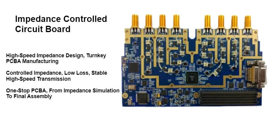
APTPCB is a vertically integrated factory that manufactures impedance-controlled PCBs and provides full turnkey PCB assembly. Because we control both bare-board fabrication and assembly operations, we align stack-up engineering, material selection, lamination and etch compensation with real assembly constraints (placement, reflow, and test). Our advantage is practical continuity: field-solver validated stack-ups, production-proven dielectric data, process compensation rules, AOI/flying-probe inspection, and impedance verification — all applied within the same production flow to ensure boards and assemblies meet signal-integrity targets with repeatable yield.
In this guide you’ll learn what impedance-controlled PCBs are, how trace geometry and materials set impedance, why manufacturers tune stack-ups and widths for production, and how partnering early with a PCB+PCBA factory minimizes layout iterations and shortens development schedules.
Table of Contents
- Understanding Impedance-Controlled PCBs in High-Speed Designs
- How Geometry and Materials Define PCB Impedance
- Why PCB Manufacturers Adjust Stack-Ups and Trace Widths
- Why You Should Involve Your PCB Manufacturer Early
- Partnering with APTPCB for High-Speed, Impedance-Controlled PCBs
Understanding Impedance-Controlled PCBs in High-Speed Designs
In low-speed circuits, a “trace is just a wire.” But once rise times get short and data rates increase, every trace becomes a transmission line with a characteristic impedance. If that impedance does not match the driver and receiver, part of the signal is reflected back along the trace—just like an echo in an empty room.
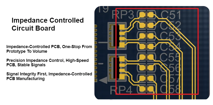
An impedance-controlled PCB is one where selected traces are designed and manufactured to a specific characteristic impedance (for example, 50 Ω single-ended or 90–100 Ω differential) within a defined tolerance. This is essential for many modern standards: USB, HDMI, PCIe, Ethernet, LVDS, high-speed ADC interfaces, and more.
Uncontrolled impedance in these systems leads to reflections, overshoot, undershoot, jitter, and EMI problems that can be difficult—or impossible—to fix later in firmware or layout tweaks.
Key Reasons Impedance Control Matters
Signal Integrity and Waveform Quality
Controlled impedance ensures that high-speed signals see a consistent transmission environment, minimizing reflections that distort eye diagrams and logic thresholds.Timing and Jitter Performance
Stable impedance reduces ringing and overshoot, improving edge fidelity and lowering jitter—critical for multi-gigabit links and tight timing budgets.Electromagnetic Compatibility (EMC/EMI)
Poor impedance control can cause excess radiation and coupling. Properly matched lines and return paths help keep emissions and susceptibility under control.Standards Compliance
Many high-speed protocols assume a specific line impedance. Meeting these assumptions at the PCB level is essential to pass compliance tests and interoperability checks.Design Predictability and Debug Simplicity
When line impedance is well controlled and documented, engineers can trust simulation results and spend less time chasing random signal-integrity issues on the bench.
Consistent Performance and Reliability
By treating impedance control as a design requirement, not a post-processing step, APTPCB helps OEMs achieve stable, repeatable behavior across prototypes, pilot builds, and mass production. Every impedance-controlled PCB is backed by defined stack-ups, process controls, and test strategies that maintain signal integrity throughout the product’s life.
How Geometry and Materials Define PCB Impedance
Impedance control is not magic—it’s the result of carefully selected trace geometry, layer stack-up, and material properties. For a given frequency range and signaling standard, we need to design the traces as either microstrip (outer layer) or stripline (inner layer) structures with well-defined dimensions and dielectrics.
The characteristic impedance of a trace is determined by how its electric and magnetic fields interact with surrounding copper and dielectric. This is why line width, copper thickness, dielectric thickness, and dielectric constant are all critical.
Key Factors That Influence PCB Impedance
Trace Width (W)
- Wider traces generally result in lower impedance; narrower traces result in higher impedance (with all other factors held constant).
- In practice, W is one of the primary tuning parameters used to hit a target impedance.
Trace Thickness (T)
- Thicker copper slightly reduces impedance due to increased conductor area.
- Standard copper weights (e.g., 0.5 oz, 1 oz) must be considered when calculating and controlling impedance.
Dielectric Height (H)
- The distance between the signal trace and its reference plane (ground or power) strongly affects impedance.
- Larger H generally increases impedance; smaller H decreases it.
Dielectric Constant (εr) of the PCB Material
- Higher εr reduces impedance; lower εr increases it.
- The effective εr can vary with resin content, frequency, temperature, and even lot-to-lot differences.
Reference Planes and Return Path Quality
- A solid, continuous reference plane under (microstrip) or around (stripline) the trace is essential for predictable impedance and clean return currents.
- Discontinuities, voids, or splits in planes can create local impedance variations and radiation.
Solder Mask and Surface Effects
- For outer-layer microstrips, the solder mask thickness and its dielectric constant slightly influence impedance.
- In fine-tuned designs, this effect is included in field-solver models for better accuracy.
Behind the scenes, impedance is often calculated using 2D field solvers (e.g., Polar tools) that consider all these variables. The PCB manufacturer then translates those calculations into realistic trace widths and stack-ups that can be built with their actual materials and processes.
Consistent Performance and Reliability
By aligning theoretical impedance calculations with real-world material data and process capabilities, APTPCB ensures that modeled impedance and measured impedance stay closely matched. This alignment is critical to maintain signal integrity across different builds, production lots, and operating conditions.
Why PCB Manufacturers Adjust Stack-Ups and Trace Widths
When you send a design with impedance requirements to a PCB shop, a professional manufacturer like APTPCB will not simply “copy” your nominal dimensions. Instead, our engineering team performs an impedance feasibility review and may suggest changes to stack-up, prepreg selection, or line widths.
This is not a challenge to your design skills; it’s a necessary step to bridge the gap between ideal calculations and practical manufacturing reality.
Key Reasons Stack-Ups and Widths Are Adjusted
Real Material Properties vs. Datasheet Values
- The dielectric constant (εr) given in laminate datasheets is often a nominal value at a specific frequency and test method.
- Actual εr in production can vary with frequency, resin content, temperature, humidity, and batch. APTPCB uses measured or statistically verified values from our own process experience to calculate impedance more accurately.
- Prepreg thickness after lamination is influenced by pressure, temperature, resin flow and copper pattern density. We use our lamination data to target realistic dielectric heights (H), not just catalog numbers.
Manufacturing Tolerances and Process Limits
- Every shop has minimum trace/space and drill size limits defined by its equipment and process capability. If your requested line width or spacing is below stable capability, we will recommend adjustments.
- Etching tolerances cause actual line widths to deviate from nominal. APTPCB compensates for this by building in appropriate margins and process controls.
- Registration tolerances in multilayer builds affect the exact position of traces relative to reference planes, which in turn impacts impedance.
Yield, Cost, and Standardization Considerations
- Extremely narrow or “exotic” line geometries may be technically feasible, but they can significantly reduce yield and raise cost.
- APTPCB maintains a set of standard stack-ups and material combinations that are proven, stable, and cost-effective. Using these as a baseline, we adjust trace widths to hit your target impedance while keeping the build robust and economical.
- Non-standard materials or thicknesses may add lead time and cost; often the same impedance can be achieved more efficiently with standard materials and tuned geometries.
In practice, the two most common adjustment levers are trace width (W) and dielectric height (H), because they have the strongest impact on impedance and can be controlled reliably in production.
Consistent Performance and Reliability
By revisiting the stack-up and geometry with realistic process data, APTPCB ensures that impedance-controlled PCBs are not only correct on paper, but also repeatable on the manufacturing floor. This reduces re-spins, improves yield, and delivers boards that behave as your simulations and lab measurements expect.
Why You Should Involve Your PCB Manufacturer Early
Given the interaction between design intent, material behavior, and process capability, the most efficient impedance-controlled PCB projects are the ones where designers and manufacturers collaborate from the beginning, not just at the Gerber handoff.
Talking to your PCB manufacturer early can turn impedance control from a “risk” into a competitive advantage—shorter development time, fewer surprises, and more predictable performance.
Key Benefits of Early Collaboration on Impedance-Controlled Designs
Access to Real Stack-Up and Material Data
- Your PCB partner can provide current, production-proven data for dielectric constants, copper thicknesses, and finished dielectric heights.
- This allows you to run more accurate simulations and avoid guessing about stack-up details.
Alignment with Process Capability
- Understanding the manufacturer’s minimum trace/space, drill size, and layer-count limits ensures your design is manufacturable from day one.
- You can avoid routing yourself into corners that require last-minute changes to meet factory constraints.
Joint Stack-Up Optimization
- APTPCB’s engineers can propose stack-ups that balance impedance targets, layer count, cost, and yield using standard materials where possible.
- We can model single-ended and differential impedances with field solvers and share target line widths per layer.
Reduced Design Iterations and Schedule Risk
- Early DFM and impedance review helps avoid multiple layout re-spins caused by manufacturability or impedance deviations discovered too late.
- This directly compresses the time from initial concept to a passing prototype.
Improved System-Level Performance and Reliability
- When layout, materials, and manufacturing process are aligned, your PCB behaves as intended across temperature, voltage, and production variability.
- This supports higher data rates, cleaner compliance margins, and fewer field issues.
Balanced Cost vs. Performance
- By optimizing impedance with realistic geometries and standard materials, we can maintain high performance without overspecifying exotic laminates or overly tight tolerances that drive cost.
What to Prepare Before Talking to Your Manufacturer
- Target impedances (e.g., 50 Ω single-ended, 90 Ω / 100 Ω differential) and which nets or interfaces require control
- Desired layer count and any constraints on board thickness or mechanical envelope
- Preferred materials (if any) or performance requirements (frequency range, loss budget, environment)
- Approximate routing density and minimum feature sizes you expect to use
Consistent Performance and Reliability
Early engagement turns the PCB manufacturer into an extension of your engineering team. At APTPCB, we use this collaboration to anchor your design in realistic stack-ups and process windows, so the first prototypes are already close to what you need for production—saving both time and budget.
Partnering with APTPCB for High-Speed, Impedance-Controlled PCBs
Impedance-controlled PCBs are no longer a niche requirement—they’re the baseline for most modern high-speed digital and RF designs. Getting them right requires more than a calculator; it requires a manufacturing partner who understands how field theory, materials, and process capability come together on the production line.
APTPCB provides:
- High-speed stack-up design support for single-ended and differential impedance
- Verified material data and standard stack-up libraries
- Field-solver-based impedance calculations and recommendations
- Process controls and test methods for impedance consistency
- Integrated PCB and PCBA services for complete, high-speed assemblies
Why OEMs Choose APTPCB for Impedance-Controlled PCBs
- Engineering-Driven Approach: We treat controlled impedance as a system requirement, not a checkbox, and support you from concept to volume.
- Realistic, Production-Ready Stack-Ups: Our stack-ups and line-width recommendations are based on actual lamination and etching behavior, not just datasheet assumptions.
- High-Yield Manufacturing: Mature processes and quality control help keep impedance within tolerance while maintaining strong yields.
- Shorter Development Cycles: Early DFM and impedance consultation reduces the number of layout iterations and surprises at the prototype stage.
- Long-Term Reliability: Stable impedance and controlled return paths support better EMI performance, timing margins, and product lifetime.
Consistent Performance and Reliability
By partnering with APTPCB for impedance-controlled PCB design and manufacturing, you gain a reliable backbone for your high-speed systems. From the first stack-up proposal to full-scale production, we help ensure that every board delivers the signal integrity, timing, and EMC performance your application demands.