Contents
- The Context: What Makes Inner Layer Etching Control Challenging
- The Core Technologies (What Actually Makes It Work)
- Ecosystem View: Related Boards / Interfaces / Manufacturing Steps
- Comparison: Common Options and What You Gain / Lose
- Reliability & Performance Pillars (Signal / Power / Thermal / Process Control)
- The Future: Where This Is Going (Materials, Integration, Ai/automation)
- Request a Quote / DFM Review for Inner Layer Etching Control (What to Send)
- Conclusion
This scenario highlights the critical nature of inner layer etching control. In the world of multilayer PCB fabrication, this process is the chemical sculpting of the internal nervous system of the board. It involves the precise removal of unwanted copper from the core laminate to define the circuit patterns—traces, pads, and planes—before the layers are pressed together.
What does "good" look like in this context? It is not merely about electrical continuity. Successful inner layer etching control delivers consistent trace geometries with vertical sidewalls (high etch factor), uniform copper distribution to prevent warping, and absolute dimensional stability to ensure layers align perfectly during lamination. It is the difference between a board that functions and a board that performs.
Highlights
- Etch Compensation: How fabricators modify artwork to counteract the "undercut" effect of chemical etchants.
- Chemistry Management: The balance between etch rate, pH, and specific gravity in Cupric Chloride systems.
- Signal Integrity Impact: The direct correlation between trapezoidal trace shapes and impedance mismatches.
- Verification: The role of Automated Optical Inspection (AOI) in catching defects before they are buried forever.
The Context: What Makes Inner Layer Etching Control Challenging
The fabrication of a Printed Circuit Board (PCB) is a sequence of chemical and mechanical steps, but the inner layer etching process is unique because it happens on thin, flexible core materials that are difficult to handle. As electronics shrink, the margin for error in etching has vanished.
The Density Dilemma
In the past, a 10-mil trace width was standard. Today, High-Density Interconnect (HDI) designs frequently demand 3-mil or even 2-mil trace widths. When etching a 3-mil line, a lateral erosion (undercut) of just 0.5 mil represents a 16% reduction in trace width. This sensitivity requires an entirely different level of process control compared to legacy manufacturing.
The "Puddle Effect"
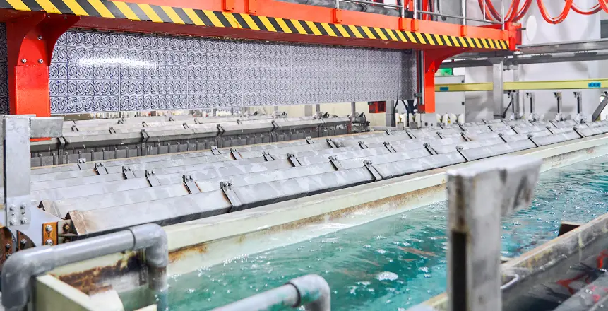
Etching is typically done in a horizontal conveyorized machine where chemical spray nozzles attack the copper. However, chemistry behaves differently on the top of the panel versus the bottom. On the top surface, fresh etchant can pool (the "puddle effect"), slowing down the reaction rate compared to the bottom side, where gravity clears the old chemistry instantly. Fabricators must use complex fluid dynamics—oscillating nozzles and specific pressure adjustments—to ensure the top and bottom etch at the exact same rate.
Material Constraints
The core material itself poses a challenge. A 4-layer board might use a rigid 0.5mm core, but a 20-layer board might use cores as thin as 0.05mm (2 mils). These thin cores are flimsy. Transporting them through high-pressure spray chambers without jamming or wrinkling requires specialized transport systems. Furthermore, the copper foil creates stress; as copper is etched away, the internal stress of the laminate is released, causing the material to shrink or stretch. APTPCB (APTPCB PCB Factory) utilizes advanced scaling algorithms to predict this movement and adjust the artwork beforehand, ensuring that after etching, the pads land exactly where they are supposed to be.
The Core Technologies (What Actually Makes It Work)
Achieving precise inner layer etching control is not about dumping panels into a bath of acid. It is a highly controlled, feedback-loop-driven process involving several core technologies.
1. The Des Line (Develop, Etch, Strip)
The heart of inner layer processing is the DES line.
- Develop: The photoresist (which was exposed to UV light through the artwork) is developed. Unexposed resist washes away, revealing the copper to be removed.
- Etch: The panel enters the etch chamber. For inner layers, Cupric Chloride (CuCl2) is the standard etchant because it offers a steady etch rate and can be easily regenerated. The chemistry attacks the exposed copper.
- Strip: The remaining hardened photoresist, which protected the circuitry, is stripped away, leaving clean copper traces.
2. Etch Compensation (the "Grow" Factor)
Chemicals etch in all directions—downwards and sideways. To etch a trace that is 1 oz (1.4 mils) thick, the chemical will also eat sideways into the trace wall. This is called "undercut." To fix this, engineers apply etch compensation to the CAM data. If the designer wants a 5-mil line, and the process has a 1-mil undercut, the fabricator will modify the film to print a 6-mil line. During etching, the 6-mil line shrinks back to the desired 5 mils. This compensation factor varies based on copper thickness, trace density, and the specific etch machine being used.
3. Automatic Dosing and Regeneration
In a high-volume environment, the chemical potency of the etchant drops as it dissolves copper. If the etchant becomes weak, the etch rate slows down, leading to under-etching (shorts). If it is too strong, it leads to over-etching (opens or thin traces). Modern lines use auto-dosing systems that continuously measure the Specific Gravity (SG) and Oxidation-Reduction Potential (ORP) of the solution. When levels drift, the system automatically injects hydrochloric acid, oxidizers, or water to maintain a steady state. This ensures that the first panel of the day and the last panel of the day receive the exact same chemical treatment.
4. Automated Optical Inspection (AOI)
Once the inner layers are etched, they are visually inspected. However, human eyes cannot reliably check millions of connections on a 3-mil pitch. AOI machines scan the copper pattern using high-resolution cameras and compare it against the original Gerber data. AOI looks for:
- Open circuits: Broken traces.
- Short circuits: Unwanted copper bridging two tracks.
- Mouse bites: Nicks in the side of a trace that reduce its width.
- Dish-down: Where the copper is thinned but not broken. Catching these defects now is mandatory. Once the layers are laminated into a multi-layer structure, repair is impossible.
Ecosystem View: Related Boards / Interfaces / Manufacturing Steps
Inner layer etching does not happen in a vacuum. It is deeply interconnected with the upstream design and downstream assembly processes.
The Link to Lamination
After etching and inspection, the copper surface is too smooth to bond well with the prepreg (glue) layers. The inner layers must go through an "oxide" or "brown oxide" treatment. This chemical process grows microscopic crystals on the copper surface, increasing the surface area and creating a "velcro-like" texture for the resin to grip. If the etching process leaves residues or uneven surfaces, the oxide coating will fail, leading to delamination (layer separation) during reflow soldering.
Impact on Drilling and Registration
The etching process releases stress in the laminate material, causing it to shrink or expand slightly. If this movement is not consistent, the PCB drilling machine—which relies on a fixed coordinate system—will miss the center of the pads. This is known as "breakout." High-layer-count boards require "scaling" data, where the fabricator intentionally prints the image slightly larger or smaller to account for the material's movement during etching.
High-Frequency Implications
For high-frequency PCBs, the shape of the etched trace is paramount. At 20GHz+, the current travels on the "skin" of the conductor. If the etching process leaves a rough, jagged edge, the signal path effectively becomes longer and more resistive due to the "skin effect." Advanced etching control for RF boards often involves slower etch speeds and specialized chemistry to ensure the smoothest possible sidewalls.
Comparison: Common Options and What You Gain / Lose
Designers often face trade-offs regarding copper weight and trace geometry. The physics of etching dictates that you cannot have both extremely thick copper and extremely fine lines without significant cost or compromise.
When you choose thicker copper (e.g., 2 oz or 3 oz) for power handling, the etching process takes longer. The longer the chemical sits on the board to cut through the vertical thickness, the longer it has to eat sideways (undercut). This limits how close traces can be to each other. Conversely, starting with thinner foil (e.g., 1/2 oz or 1/3 oz) allows for very fine lines but limits current capacity.
Decision Matrix: Technical Choice → Practical Outcome
| Technical choice | Direct impact on Etching & Design |
|---|---|
| Heavy Copper (2oz+) | Requires larger spacing (min 8-10 mil). Significant undercut; trace shape becomes trapezoidal, affecting impedance. |
| Standard Copper (1oz) | Balanced performance. Standard 4-5 mil trace/space is easily achievable with good yield and vertical sidewalls. |
| Thin Copper (1/3oz or H oz) | Enables HDI features (3mil/3mil). Very fast etch time reduces undercut, providing excellent impedance control. |
| Vacuum Etching | Advanced technique that sucks spent etchant out of fine gaps. Essential for < 3mil spaces to prevent "puddle" blockage. |
Reliability & Performance Pillars (Signal / Power / Thermal / Process Control)
The quality of the inner layer etch directly dictates the reliability of the final product. APTPCB focuses on three main pillars of performance that are determined at this stage.
1. Signal Integrity and Impedance
For controlled impedance lines (e.g., USB, PCIe, DDR), the trace width is the most critical variable. A 10% reduction in trace width can increase impedance beyond the allowable tolerance. However, it is not just the width at the top of the trace; it is the cross-sectional area. Etching naturally creates a trapezoidal shape (wider at the bottom, narrower at the top). If the "etch factor" (the ratio of downward etch to sideways etch) is poor, the trace becomes very triangular. This reduces the effective copper volume, increasing DC resistance and altering the electromagnetic field coupling to the reference plane. Using an impedance calculator during the design phase helps, but the fabricator must hit the target geometry physically.
2. Thermal Reliability
In power electronics, neck-down—a localized narrowing of a trace due to over-etching or a "mouse bite" defect—creates a hotspot. Under high current loads, this narrow point acts like a fuse. Over time, thermal cycling at this hotspot can cause the copper to crack or delaminate from the resin. Consistent etching ensures that the current-carrying capacity is uniform across the entire length of the conductor.
3. Inter-Layer Insulation
Under-etching is a silent killer. If the copper is not completely removed from the spaces between traces, it can leave behind a thin, invisible film of conductive residue (sometimes called "copper foot"). This might pass a low-voltage electrical test but can cause leakage currents or arcing under high-voltage operation. Thorough rinsing and "stripping" processes are required to ensure the insulation resistance between tracks is absolute.
Acceptance Criteria Example
| Feature | Standard Spec | Advanced Spec |
|---|---|---|
| Trace Width Tolerance | +/- 20% | +/- 10% or +/- 1 mil |
| Min Etch Factor | 2:1 | 3:1 or higher |
| Defects (Open/Short) | 0 allowed | 0 allowed |
| Line Edge Roughness | < 0.5 mil | < 0.2 mil (for RF) |
The Future: Where This Is Going (Materials, Integration, Ai/automation)
The traditional "subtractive" etching process (start with full copper, remove what you don't want) is hitting physical limits. As we push towards 1-mil lines and spaces for semiconductor packaging substrates, the industry is evolving.
One major shift is toward Modified Semi-Additive Processes (mSAP). Instead of etching away thick copper, mSAP starts with a very thin seed layer, uses a photoresist to define the negative image, and then plates the copper up into the channels. The etching step is then only used to remove the ultra-thin seed layer at the end. This allows for perfectly rectangular trace geometries that subtractive etching cannot achieve.
Additionally, Artificial Intelligence is revolutionizing the AOI verification step. Traditional AOI relies on strict algorithms that often flag false errors (e.g., oxidation spots looking like opens). AI-driven AOI learns from thousands of panels to distinguish between a harmless cosmetic blemish and a functional defect, improving throughput and reducing manual verification errors.
5-Year Performance Trajectory (Illustrative)
| Performance metric | Today (typical) | 5-year direction | Why it matters |
|---|---|---|---|
| Min Trace/Space (Subtractive) | 3 mil / 3 mil | 2 mil / 2 mil | Higher density for mobile/wearable devices without moving to mSAP cost structures. |
| Etch Tolerance | +/- 10-15% | +/- 5% | Critical for 112G and 224G SerDes signal integrity requirements. |
| Etchant Chemistry | Standard Cupric Chloride | Closed-loop Regenerative | Zero-discharge environmental compliance and reduced chemical costs. |
Request a Quote / DFM Review for Inner Layer Etching Control (What to Send)
When requesting a quote for a multilayer board where impedance and etching precision are critical, providing a complete data package allows the engineering team to apply the correct compensation factors immediately. A generic request may lead to standard tolerances that are insufficient for high-speed designs.
Checklist for High-Precision Etching Quotes:
- Gerber Files (RS-274X): Ensure all inner signal and plane layers are included.
- Stackup Diagram: Clearly specify the core thickness and copper weight (e.g., "0.1mm core, H/H oz copper").
- Impedance Table: List the target impedance (e.g., 50Ω SE, 100Ω Diff) and the specific layers/traces involved.
- Material Type: Specify if High-Tg or Low-Loss material (like Rogers or Megtron) is required, as this affects etch rates.
- Minimum Trace/Space: Explicitly state the tightest geometry on the board (e.g., "3.5 mil trace / 4 mil space").
- Netlist (IPC-356): Essential for verifying that the etched inner layers match the electrical logic before lamination.
Conclusion
Inner layer etching control is the defining process that transforms a sheet of copper-clad laminate into a functional electronic circuit. It is a discipline that balances chemical aggression with microscopic precision, ensuring that the millions of connections inside a modern PCB are geometrically accurate and electrically sound.
As designs continue to push the boundaries of density and speed, the "art" of etching is becoming a rigorous science of fluid dynamics and chemical engineering. By understanding these constraints and collaborating with a capable manufacturer like APTPCB early in the design phase, engineers can ensure their complex multilayer boards are built on a foundation of reliability.