
Designing a Key Fob PCB presents a unique engineering paradox: the device must be incredibly small and inexpensive, yet it must perform reliably in harsh RF environments while running for years on a single coin cell battery. Unlike standard consumer electronics, a key fob cannot fail when dropped on concrete or exposed to rain. This guide provides the specific layout rules, material specifications, and troubleshooting steps required to manufacture high-reliability remote keyless entry (RKE) and passive keyless entry (PKE) circuits.
APTPCB (APTPCB PCB Factory) specializes in the precision manufacturing required for these compact, high-density boards. Whether you are designing a simple garage door opener or a complex encrypted automotive smart key, the physical constraints of the enclosure dictate the electrical strategy.
Quick Answer (30 seconds)
For a functional and durable Key Fob PCB, adhere to these core engineering boundaries immediately.
- Frequency Matching: Ensure the antenna geometry matches the target frequency (commonly 315 MHz, 433.92 MHz, or 868 MHz) inside the final plastic enclosure, as the casing shifts the resonant frequency.
- Battery Contact Plating: Use Hard Gold (not ENIG) for battery contact pads to prevent fretting corrosion from the coin cell holder.
- Standby Current: The total system quiescent current must be below 1µA to ensure a 3-5 year battery life on a CR2032.
- PCB Thickness: Standard 1.6mm is often too thick; utilize 0.8mm or 1.0mm FR4 to accommodate buttons and battery holders within the slim profile.
- Button Placement: Tactile switches must be placed exactly opposite to the battery or structural ribs to prevent PCB flexing during actuation.
- RF Isolation: Keep the crystal oscillator and digital lines at least 3mm away from the antenna trace to minimize harmonic noise.
When Key Fob PCB applies (and when it doesn’t)
Determining if your project follows "Key Fob" design rules depends on power constraints and form factor, not just the device name.
This design approach applies when:
- Space is the primary constraint: The PCB outline is non-rectangular and tightly follows the curvature of a handheld enclosure.
- Power is finite: The device runs on a coin cell (CR2032, CR2025) and spends 99% of its life in deep sleep mode.
- RF is integrated: The antenna is a PCB trace (loop or F-antenna) rather than an external SMA connector or ceramic chip (due to cost).
- Durability is critical: The board must withstand high G-force impacts from being dropped on keys.
- Cost sensitivity is high: The BOM must be minimized, often eliminating shielding cans in favor of clever layout isolation.
This design approach does not apply when:
- Continuous Data Streaming: Devices like a 360 Degree Camera PCB or 4K Camera PCB require high-speed differential pairs and thermal management that key fobs do not.
- Rechargeable High Power: If the device uses a Li-Po battery with a charging circuit, the power management layout differs significantly from coin-cell logic.
- Long Range Telemetry: LoRa or Sigfox trackers requiring kilometers of range usually require larger ground planes than a key fob can provide.
- High Processing Load: If the device runs a Linux OS or processes video, it is not a key fob architecture.
Rules & specifications
The following table outlines the critical parameters for manufacturing a Key Fob PCB. Deviating from these values often leads to mechanical failure or poor RF range.
| Rule | Recommended Value/Range | Why it matters | How to verify | If ignored |
|---|---|---|---|---|
| PCB Thickness | 0.8mm to 1.0mm | Reduces vertical stack-up height to fit slim enclosures. | Caliper measurement on bare board. | Enclosure won't snap shut; buttons permanently pressed. |
| Copper Weight | 1 oz (35µm) | Provides mechanical strength for battery contacts and button pads. | Microsection analysis. | Pads peel off after repeated battery replacements. |
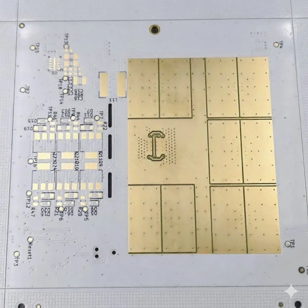
| Surface Finish | Hard Gold (or Immersion Silver) | Hard Gold resists wear from battery friction; Silver is good for RF. | X-Ray Fluorescence (XRF). | Contact oxidation leads to intermittent power failure. |
| Antenna Clearance | > 5mm from ground pour | Copper near the antenna detunes it and absorbs energy. | Gerber viewer (Keep-out layers). | Drastically reduced transmission range (< 5 meters). |
| Via Stitching | < λ/20 spacing | Creates a Faraday cage effect around RF sections to block noise. | Visual inspection of ground pour edges. | Digital noise couples into the RF carrier; signal jitter. |
| Solder Mask Color | Matte Green or Blue | Glossy black can be difficult for AOI; Matte reduces solder bridging visibility issues. | Visual inspection. | Higher defect rate during assembly inspection. |
| Trace Width (RF) | 50Ω Impedance Matched | Ensures maximum power transfer from transceiver to antenna. | Impedance Calculator | Signal reflects back to the chip; poor range. |
| Button Pad Size | +0.5mm over component | Allows for slight misalignment during pick-and-place. | Footprint verification in CAD. | Weak solder joints on frequently pressed buttons. |
| Crystal Layout | < 5mm trace length | Long traces act as antennas for clock noise. | Measure distance in layout software. | Radiated emissions fail FCC/CE certification. |
| Test Points | 1.0mm diameter pads | Essential for pogo-pin programming and fixture testing. | Overlay with test fixture design. | Cannot program firmware or test RF in production. |
| Panelization | V-Score or Mouse Bites | Small boards are hard to handle individually; panels improve assembly speed. | Check panel drawing. | High assembly cost; irregular board edges. |
| Conformal Coating | Acrylic or Silicone | Protects against sweat, rain, and pocket lint moisture. | UV light inspection (if tracer added). | Corrosion causes shorts after 3-6 months of use. |
Implementation steps

Designing a Key Fob PCB requires a specific workflow that prioritizes the mechanical constraints first, followed by the RF performance.
1. Mechanical Outline & Constraint Definition Before drawing a single schematic wire, import the DXF file of the enclosure into your PCB CAD tool. Define the exact locations of mounting bosses, button actuators, and the battery cavity. The PCB outline usually requires complex curves.
- Action: Define "Keep-out" zones where the plastic ribs of the case will touch the PCB.
- Check: Verify the battery holder fits without hitting the top cover.
2. Schematic Design for Low Power Select components with the lowest quiescent current (Iq). Use high-value pull-up/pull-down resistors (e.g., 1MΩ instead of 10kΩ) to minimize leakage.
- Action: Choose a microcontroller with a deep sleep mode < 500nA.
- Check: Calculate the total theoretical standby current.
3. Component Placement (The "RF First" Rule) Place the RF transceiver and antenna matching network first. They require the cleanest area of the board.
- Action: Place the crystal oscillator as close to the MCU pins as possible. Place the battery holder on the bottom side (usually) to save top-side space for buttons.
- Check: Ensure the antenna area is free of copper on all layers.
4. RF Routing and Impedance Control Route the RF trace from the transceiver to the antenna using a calculated width for 50Ω impedance.
- Action: Use a coplanar waveguide structure (ground plane on both sides of the trace) if space permits. Use APTPCB tools to verify stack-up.
- Check: Ensure no digital lines cross under the RF trace.
5. Ground Plane Strategy A solid ground plane is essential for the antenna to work (it acts as the counterpoise).
- Action: Pour a solid ground plane on the bottom layer. Stitch top and bottom grounds together with vias, especially near the RF section.
- Check: Ensure the ground plane is not cut into islands by long signal traces.
6. Prototyping and Tuning Order a small batch of prototypes. The antenna will likely be detuned.
- Action: Use a Vector Network Analyzer (VNA) to measure the antenna match with the plastic case on. Adjust the matching network (capacitor/inductor values) to center the frequency.
- Check: Verify range in an open field environment.
7. Design for Manufacturing (DFM) Review Small boards often suffer from "tombstoning" (components standing up) during reflow due to thermal imbalance.
- Action: Ensure thermal relief connections are used on ground pads. Submit files to APTPCB DFM Check.
- Check: Verify panelization tabs do not interfere with the final assembly into the case.
Failure modes & troubleshooting
Key Fob PCBs are prone to specific failures due to their usage environment. Following the "Symptom → Cause → Fix" logic helps resolve these quickly.
1. Symptom: Short Transmission Range (< 5 meters)
- Cause: Antenna detuning. The plastic case or the user's hand shifts the resonant frequency.
- Check: Measure RSSI (Received Signal Strength Indicator) with and without the case.
- Fix: Retune the matching network values while the PCB is inside the housing.
- Prevention: Leave more clearance between the antenna trace and nearby components/ground.
2. Symptom: Battery Drains in Weeks (Not Years)
- Cause: "Stuck" button or firmware sleep failure. Moisture causing micro-shorts.
- Check: Measure current draw. If it fluctuates, the MCU isn't sleeping. If constant high draw, check for shorts.
- Fix: Add conformal coating. Check switch mechanical tolerance (is the case pressing the button?).
- Prevention: Use interrupts for button presses rather than polling loops in firmware.
3. Symptom: Intermittent Operation when Pressed Hard
- Cause: PCB flexing or cracked solder joints.
- Check: Inspect the solder joints of the battery holder and switches under a microscope.
- Fix: Increase pad size. Add support ribs in the enclosure behind the buttons.
- Prevention: Use 1.0mm thickness instead of 0.8mm if the enclosure allows.
4. Symptom: Device Resets when Dropped
- Cause: Battery bounce. The coin cell momentarily disconnects upon impact.
- Check: Drop test the device while monitoring the power rail with an oscilloscope.
- Fix: Add a large bulk capacitor (e.g., 100µF tantalum) across the power rail to bridge the gap.
- Prevention: Use a battery holder with higher retention force or a dual-contact design.
5. Symptom: LED Lights Up but No Signal Received
- Cause: Crystal oscillator failure or frequency drift.
- Check: Measure the carrier frequency with a spectrum analyzer.
- Fix: Replace the crystal. Check load capacitance (CL) values.
- Prevention: Ensure the crystal is rated for the shock/vibration specifications of a key fob.
6. Symptom: Corrosion on Battery Pads
- Cause: Galvanic reaction between the battery casing and PCB finish.
- Check: Visual inspection for green/black residue.
- Fix: Switch surface finish to Hard Gold.
- Prevention: Avoid touching pads with bare fingers during assembly; seal the enclosure better.
Design decisions
When moving from a standard PCB to a Key Fob PCB, or even denser technologies like a 360 Degree Camera PCB, the density of the interconnects drives the cost and complexity.
HDI vs. Standard Through-Hole Most key fobs can be designed using standard through-hole technology (Type I or II), keeping costs low. However, if the key fob includes a display or biometric sensor, you may need High Density Interconnect (HDI) techniques similar to those used in a 4K Camera PCB.
- Standard Key Fob: 2-layer, 0.2mm vias, 5/5 mil trace/space. Low cost, high yield.
- Advanced Smart Key: 4-layer, blind vias, 3/3 mil trace/space. Required for BGA microcontrollers or secure element chips.
Material Selection: FR4 vs. Rogers While standard FR4 is sufficient for 315/433 MHz, attenuation becomes an issue at higher frequencies (2.4 GHz for Bluetooth Low Energy fobs).
- Decision: For standard RKE, use high-Tg FR4. For BLE or UWB (Ultra Wide Band) fobs used in modern cars, consider Rogers or Megtron materials for the RF layers to preserve signal integrity.
Antenna Type: PCB Trace vs. Chip
- PCB Trace (Loop/F-Type): Free (zero BOM cost), but requires large board area and is sensitive to layout. Best for high-volume, low-cost fobs.
- Chip Antenna: Costs money ($0.10 - $0.50), but is smaller and less sensitive to detuning. Best for ultra-compact designs where board space is premium.
FAQ
1. What is the best PCB thickness for a key fob? The industry standard is 0.8mm or 1.0mm. This saves vertical space for the battery and buttons. 1.6mm is usually too thick for modern slim enclosures.
2. Can I use a PCB trace antenna for 433 MHz? Yes, a printed loop antenna is very common. However, at 433 MHz, the wavelength is long (~70cm), so the antenna is electrically "small" and inefficient. It requires careful impedance matching to work effectively.
3. Why does my key fob range drop when I put it in the case? Plastic has a dielectric constant different from air. This changes the capacitance around the antenna, shifting its resonant frequency. You must tune the antenna inside the case.
4. How do I waterproof a Key Fob PCB? You cannot easily seal the battery door perfectly. The best approach is applying a conformal coating (acrylic or silicone) to the PCB assembly, leaving only the battery contact points exposed.
5. Should I use ENIG or HASL finish? Avoid HASL for fine-pitch components. ENIG is good, but Hard Gold is best for the battery contacts because it withstands the friction of battery insertion and removal better than ENIG.
6. How do I extend the battery life of my design? Focus on the "sleep" current. The MCU should be in deep sleep (nA range) 99.9% of the time. Also, avoid LEDs that are too bright; a 2mA LED is sufficient for indication.
7. What is the difference between RKE and PKE? RKE (Remote Keyless Entry) transmits only when a button is pressed. PKE (Passive Keyless Entry) constantly listens for a "wake up" signal from the car, requiring a 3-axis low-frequency antenna coil on the PCB, which takes up significant space.
8. Can APTPCB manufacture flexible key fob circuits? Yes. Rigid-flex PCBs are increasingly used in premium key fobs to wrap circuits around the battery or fit into ergonomic shapes.
9. How do I prevent buttons from breaking off the PCB? Use switches with locating pegs (bosses) that fit into holes in the PCB for mechanical stability. Also, ensure the solder mask opening is sufficient for a strong solder fillet.
10. Why is impedance control important for such a short trace? Even short traces can cause reflections if the mismatch is severe. For a key fob, every decibel of power loss translates to meters of lost range. Using an impedance calculator ensures your trace width matches the transceiver's output.
11. What is the typical lead time for Key Fob PCBs? Standard prototypes take 24-48 hours. Production volumes depend on complexity but are typically 5-7 days.
12. Do I need shielding cans? For simple 433MHz fobs, usually no. For complex fobs with Bluetooth or high-speed processors, shielding may be required to pass EMC certification.
Related pages & tools
To ensure your Key Fob PCB is manufacturable and performs correctly, utilize these resources:
- PCB Manufacturing Services: Full capabilities list for rigid and rigid-flex boards.
- Gerber Viewer: Verify your antenna keep-out zones and drill hits before ordering.
Glossary (key terms)
| Term | Definition | Context in Key Fob PCB |
|---|---|---|
| RKE | Remote Keyless Entry | System where the user must press a button to unlock. |
| PKE | Passive Keyless Entry | System where the fob unlocks automatically when near the receiver. |
| Coin Cell | Lithium Manganese Dioxide Battery | The standard power source (CR2032, CR2025) providing 3V. |
| Matching Network | Circuit of capacitors/inductors | Adjusts antenna impedance to 50Ω to maximize range. |
| Detuning | Frequency Shift | When the antenna resonates at the wrong frequency due to nearby objects. |
| SAW Filter | Surface Acoustic Wave | A filter that removes noise, allowing only the specific frequency to pass. |
| Tactile Switch | Momentary Push Button | The physical interface; requires careful mechanical placement. |
| RSSI | Received Signal Strength Indicator | A metric used to measure how strong the signal is at the receiver. |
| Fretting Corrosion | Micro-motion induced wear | Oxidation on battery contacts caused by vibration, leading to power loss. |
| Keep-out Zone | Restricted Area | Area on the PCB where no copper or components should be placed (for antenna). |
| Via Stitching | Connecting ground planes | Using multiple vias to connect top and bottom grounds to shield RF. |
| Parasitic Capacitance | Unwanted energy storage | Capacitance created by PCB traces that can disrupt the crystal oscillator. |
Conclusion
Designing a successful Key Fob PCB is an exercise in balance. You must balance the physical constraints of a handheld device with the physics of RF transmission, all while maintaining a price point suitable for mass production. By adhering to strict layout rules—specifically regarding antenna clearance, battery contact durability, and power management—you can avoid the common pitfalls of short range and dead batteries.
Whether you are prototyping a new IoT tracker or scaling production for an automotive entry system, the quality of the bare board dictates the reliability of the final product. APTPCB provides the specialized fabrication techniques, from impedance control to hard gold plating, necessary to deliver high-performance compact PCBs.
Ready to prototype your design? Upload your Gerber files to our Quote Page for an instant review and pricing.